The trend of larger capacity batteries requiring the same or faster charging time is accelerating the adoption of higher power and output voltage by USB-C PDs. The USB PD organization has released the latest USB PD3.1 EPR specification, which enables the maximum output to reach 48V 5A and 240W power. When designing USB PD adapters and chargers, it is necessary to meet the latest energy efficiency standards such as COC V5 Tier2, and consider miniaturization design to match the trend of lightweight, short, but diverse functions in mobile portable devices. Onsemi‘s latest 240 W totem pole PFC, combined with the latest high-frequency quasi resonant (QR) controller, forms a dual switch flyback converter USB PD3.1 EPR adapter and fast charge reference design. The analog protocol control board supports all PD 3.1 EPR fixed outputs. Under the 230Vac and 48V output conditions, the average energy efficiency of four points reaches 95.4%. At 230Vac and 48V5A, the efficiency reaches 96.2%, and the standby power consumption is below 100mW, far exceeding the COC V5 Tier2 standard, Moreover, the PCBA is only 89mm x 51mm x 21.5mm in size, with a power density of 40W/Cubic inch and a low-cost double-layer PCB design. It is an ideal solution for the next generation PD3.1 EPR smart phone fast charging, laptop adapter, power tool fast charging, etc.
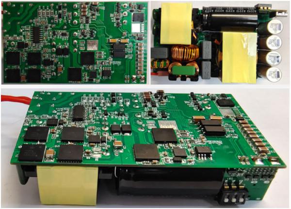
Figure 1: 40W totem pole PFC combined with high-frequency QR dual transistor flyback USB PD3.1 EPR adapter and fast charging scheme
The PFC of this scheme uses the NCP1680 CRM mode, a totem pole PFC controller with valley synchronous frequency backtracking, and an efficient PFC circuit composed of two 65mohm SJ FETs and two 50mohm iGaNs. The efficiency of the PFC is as high as 97% under 90Vac and full load conditions. In the light load mode, a skip pulse signal is generated by the downstream circuit and input to NCP1680, causing the PFC to enter the forced skip standby mode. The output voltage fluctuates between 94% and 100% of the rated value to reduce switching losses and improve light load efficiency.
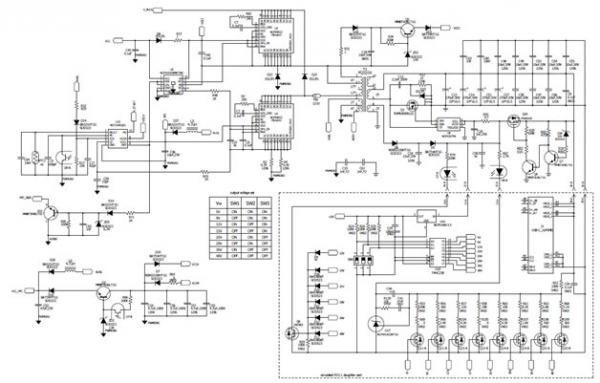
Figure 2: Schematic diagram of 240W totem pole PFC circuit
The PWM part uses the NCP1345 high-frequency QR flyback pulse width modulation (PWM) controller of Onsemi, a half bridge drive controller NCP51530 and two iGaNs to form a dual transistor flyback topology architecture, so that the transformer can adopt a large turn ratio, the power supply can work in the ZVS state approximately, and the leakage inductance energy can be fully fed back to the power input terminal to achieve very high conversion efficiency. The synchronous rectification controller NCP4307 supports high and low voltage power supply and the peripheral circuit is very simple. The output rectification adopts a 120V, 4ohm SJ FET FDMS4D0N12C.
Increasing the operating frequency can reduce the size of the power supply. This design operates in PFC with an output of 390V and full load, with a frequency of 130-150 KHz. The NCP1345 QR flyback topology uses a proprietary valley locking circuit to ensure a stable valley switch until the 6th valley. As the load further decreases, the NCP1345 enters Quiet Skip and flyback discontinuous conduction mode (DCM) during no-load and light load, and then transitions to frequency flyback mode, To reduce switch losses and improve no-load and light load energy efficiency. Bottom locking and Quiet Skip achieve market leading noise performance, and due to the reduced harmonic content of the waveform, electromagnetic interference (EMI) performance is also improved, which can reduce the required EMI filters and thus reduce costs. The inherent primary constant current control of NCP1345 makes it easy to design the maximum constant current point, which is the OCP protection value. This OCP value is almost fixed across all input and output voltage ranges. In addition, NCP1345 also provides high and low voltage dual power supply VCC terminals to simplify the design of VCC circuits.
Figure 3: Schematic diagram of 240W dual transistor flyback synchronous rectification and analog protocol control circuit
The dual transistor flyback converter requires that the design of N * Vo must be less than the input voltage, otherwise it will automatically limit the duty cycle and cause OCP protection. Therefore, in the design of the transformer‘s turn ratio, the minimum input DC voltage when N * Vo is less than 90Vac at 5V, 9V, and 12V can be ensured. This way, the PFC can be turned off at 5V, 9V, and 12V to improve efficiency. The PFC always works when the output voltage is 15V or above to ensure the normal operation of the dual transistor topology.
Due to the lack of a suitable 48V protocol controller, a 431 reference reference combined with a DIP switch discrete circuit was used to generate output voltage control sampling feedback and PFC control circuits to simulate the working state of PD3.1 EPR. All of these circuits were designed on a single sub board for future replacement of PD sub cards. The interface of the simulated PD protocol board is fully compatible with the current protocol interface. This reference design currently only supports fixed output voltage of PD3.1 EPR, and does not currently support PD3.1 EPR AVS output. Therefore, in the future, as long as a PD3.1 EPR protocol sub card is designed and installed, it can support complete PD3.1 EPR output.
Energy efficiency testing
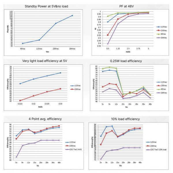
In the case of 230Vac and 5V output without load connection, the input power is less than 100mW, and the standby power consumption and PF curve at 48V are shown in the following figure. The efficiency under 5V small load and 0.25W efficiency under various outputs are also very good. The average energy efficiency and light load (10% load) energy efficiency of input voltages at 115 VAC (blue curve) and 230 VAC (red curve) are significantly higher than the COC V5 Tier 2 average energy efficiency standard and COC V5 Tier 2 light load energy efficiency standard. Due to the PFC stopping at 5V, 9V, and 12V, it can be seen that these voltages have higher efficiency, and the efficiency at 28V and 48V full load is also very high.
Figure 4: Standby Power Consumption and Energy Efficiency Curve
Figure 5: Load efficiency curves for 28V and 48V
Safety protection function and constant current control
This high-frequency QR USB PD scheme integrates rich safety and protection functions, including precise instantaneous overvoltage protection (OVP), overcurrent protection (OCP), short circuit protection (SCP), open loop protection, X2 capacitor discharge, etc.
OVP protection can be accurately set through the external resistance of the ZCD pin. OCP can set precise constant current output values through transformer turn ratio, primary current sensing resistance, and constant current voltage reference inside NCP1345. The specific design can refer to the specifications.
Thermal performance testing
Due to its high efficiency, this scheme relies on natural heat dissipation to obtain the following thermal imaging image without adding any thermal conductive materials or active heat dissipation. The thermal imaging image was measured after 30 minutes of full load operation.
Figure 6: 240W high-frequency QR USB PD3.1 EPR adapter reference design thermal imaging
|
Disclaimer: This article is transferred from other platforms and does not represent the views and positions of this site. If there is any infringement or objection, please contact us to delete it. thank you!
中恒科技ChipHomeTek
|


 Service mailbox
 13823783658
 ChatNow