Scientists at the University of Chicago in the United States have published a paper in the latest issue of Science stating that they have developed the thinnest chip level optical circuit to date - a two-dimensional (2D) waveguide. This glass crystal, which is only a few atoms thick, can capture and carry light with astonishing efficiency. It can propagate light up to a distance of one centimeter, which is a very distant distance in the field of optical computing and is expected to pave the way for new technologies.
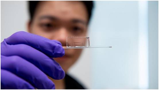
Scientists at the University of Chicago have developed a glass crystal with only a few atomic thicknesses that can capture and carry light. The picture shows the researcher holding this material. Image source: Jean Lachat/Physicist Organization Network
Guiding light from one place to another is the backbone of the modern communication world. Between the seabed and the mainland, the light transmitted by fiber optic cables encodes everything from videos to bank transfer transactions, all within strands of hair.
To make these strands thinner, even in 2D, the research team has invented a new 2D waveguide. It is a glass crystal made of molybdenum disulfide. This ultra-thin 2D crystal can not only accommodate energy, but also transmit energy to a distance 1000 times farther than existing similar systems. The captured light also behaves as if it propagates in 2D space.
The research team pointed out that it is crucial that in existing 3D waveguides, photons always propagate in a closed manner within the waveguide. However, in the new system, glass crystals are actually thinner than photons themselves, so a portion of photons will "overflow" from the crystal during propagation, making it easier to manufacture complex devices using glass crystals because light can be easily moved using lenses or prisms. In addition, photons can also "sense" information about the surrounding environment along the way, and scientists can also use these waveguides to manufacture sensors at the micro level.
Researchers are very interested in building very thin two-dimensional photonic circuits, which can be stacked in the future to integrate more small devices into the same area of the chip.
|
Disclaimer: This article is transferred from other platforms and does not represent the views and positions of this site. If there is any infringement or objection, please contact us to delete it. thank you!
中恒科技ChipHomeTek
|

 Service mailbox
 13823783658
 ChatNow