Bootstrap technology is applicable to most boost converters and can keep driving heavy loads when the voltage of the converter decreases. Many portable designs require boost converters to convert low battery voltage to higher voltage. However, as the battery voltage gradually decays, the driving force on the boost converter FET will decrease, sometimes reducing the current transmitted to the output. Bootstrap technology overcomes this problem, not only prolongs the service life of the battery, but also enhances the efficiency when driving heavy load.
These boost converters are designed to improve utility
Adp1612 is a low-cost and high-efficiency boost converter with 1.3 MHz, which is very suitable for consumer electronic circuits that must be kept small. The built-in shutdown pin can reduce the quiescent current to less than 2 μ A. It operates at an input voltage as low as 1.8 V, so it is very suitable for battery powered electronic devices. However, as the battery voltage decreases, the peak current will also decrease. It is advantageous if gentle handling is required during the last few hours of battery use, but this can lead to problems when driving a heavy load with a low battery input voltage. Bootstrap technology overcomes this problem and allows the battery voltage to be reduced to a lower level while providing high output current and high efficiency.
Extend battery life through boost converter
Figure 1 shows the standard evaluation suite of adp1612. A 200 m Ω current detection resistance is added in series with the battery input to measure the input current. A large electrolytic capacitor is added to the battery input circuit to smooth the current peak of the inductor, so that the average battery current on the detection resistance can be measured highly accurately. The battery voltage is measured by a digital voltmeter, so the input power can be calculated by multiplying the battery voltage by the input current. Add a resistive load at the output end, divide the output power by the input power, and calculate the efficiency of the converter.
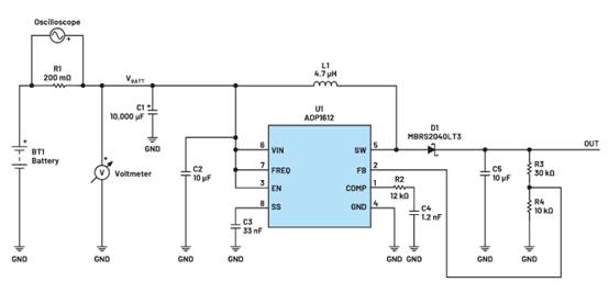
By probing the switch node (SW), we can deeply understand how the DC-DC converter works. When the FET is turned on, the inductance current increases, resulting in the increase of the bottom voltage of the switching node, and the amplitude is directly proportional to the on resistance of the FET. The lower the voltage, the lower the on resistance of the FET. Therefore, the lower the loss in the FET at a given current. Figure 2 shows a switching node in a non bootstrap configuration with a battery voltage of 2 v. The bottom voltage peak of the switching node is about 180 MV.
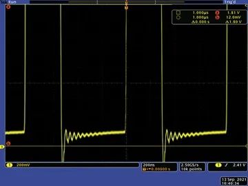
Figure 2 Switching node voltage, 2 V input, non bootstrap.
By increasing the battery voltage to 3 V, the switching node waveform shown in Fig. 3 can be obtained. We note that the duty cycle decreases as the battery voltage increases. In addition, the voltage in the lower half of the switching node is significantly lower, with a peak of about 80 mV. However, since the FET current of 3 V battery voltage is lower than that of 2 V battery voltage, it is difficult to see whether the on resistance is indeed reduced.
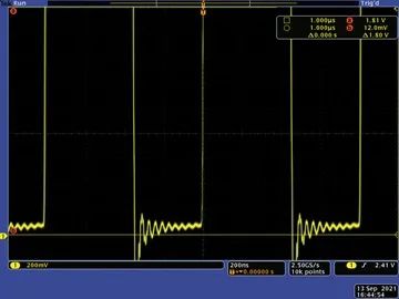
Figure 3 Switching node voltage, 3 V input, non bootstrap.
Then, the circuit shown in Fig. 1 is converted to a bootstrap configuration. Bootstrapping involves connecting the VIN pin of adp1612 to the output voltage. After this part is started, it is powered by a higher output voltage, so a stronger driving force will be generated to drive the FET, but adp1612 does not know the voltage level of the battery. The modified circuit is shown in Figure 4.
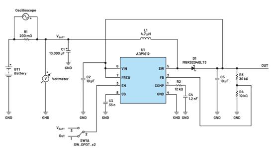
Figure 4 Bootstrap VIN pin from output voltage.
The enable pin can be connected to the battery voltage Vbatt or to the output voltage. If the battery voltage drops below about 1.7 V, connecting it to the battery voltage will set undervoltage protection (UVLO), but when connecting it to the output voltage, adp1612 can continue to switch even if the battery voltage drops far below this voltage.
Figure 5 shows the efficiency results of non bootstrap and bootstrap configurations when the battery voltage is 2 V and the measured output voltage is 4.95 v.
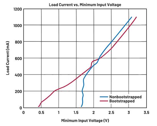
Figure 5 When the input voltage is 2 V, the efficiency of adp1612 in non bootstrap configuration and bootstrap (B / s) configuration.
In Figure 5, the efficiency curve of bootstrap configuration is represented by a solid line, which is significantly lower under light load. This is mainly because the quiescent current of the device (about 4 MA) now comes from the output voltage, which is actually multiplied by the factor
|
Disclaimer: This article is transferred from other platforms and does not represent the views and positions of this site. If there is infringement or objection, please contact us to delete. thank you!
中恒科技ChipHomeTek
|

 Service mailbox
 13823783658
 ChatNow