Hot KeyWords:CST8002D  CST6118  CST6508  XS9971   CST118S  CST2466  矽源特科技

Technology Exchange
You are here : Technology Exchange

Design of high efficiency audio power amplifier based on class D amplifier

Views:198Time:2022-06-30
    Reading Guide: in order to improve the efficiency of power amplifier and adapt to the development trend of high efficiency, energy saving and miniaturization in modern society, class D power amplifier is the core, single chip microcomputer 89C51 and programmable logic device (FPGA) are used for control and timely data processing, so as to realize the high-efficiency amplification of audio signal.

    1 system scheme demonstration and selection

    1.1 overall scheme
    Scheme ①: digital scheme. After the input signal is pre amplified and conditioned, that is, the A / D is collected into the single chip microcomputer for processing. The generation of triangular wave and the comparison with audio signal are completed by the software part, and then the single chip microcomputer outputs two completely reverse PWM waves to the power amplification part of the later stage for amplification. The hardware circuit of this scheme is simple, but it will introduce large digital noise.
    Scheme ②: hardware circuit scheme. Triangular wave generation and comparison and PWM generation are still realized by hardware circuit. This scheme has less noise, larger amplitude and better effect, so this scheme is adopted.

1.2 triangular wave generation circuit design
    Scheme ①: use NE555 to generate triangular wave. The characteristic of the circuit is that the constant current source is used to linearly impulse and discharge the capacitor to produce triangular wave. The waveform linearity is good, the frequency control is simple, and the signal amplitude can be controlled by adding an attenuation potentiometer.
    Scheme ②: triangular wave is generated by square wave integration. The integrator is cascaded with the comparator, and the triangular wave is obtained by integrating the square wave generated by the comparator. The frequency and amplitude control only needs to adjust some resistance values, so the control is simple. However, considering the existence of integral drift in the integral circuit.

Option ① is adopted here.

1.3 PWM wave generation scheme design
    Scheme ①: direct comparison. The triangular wave signal with the same bias as the input audio signal and a slightly larger amplitude is directly compared with the audio signal to generate PWM wave, and then a completely opposite PWM wave signal is generated through the inverter to the later stage amplification circuit.
    Scheme ②: two-way comparison. The two offset triangular wave signals are compared with the upper and lower half of the audio signal respectively. This scheme can reduce the opening and closing times of CMOS transistor in suffix H-bridge circuit, reduce power loss and improve efficiency.
    Scheme ③: directly reverse the audio signal. After the audio input signal is amplified and conditioned, it is directly reversed, and then the triangle wave of the processed signal is compared, so as to generate two reversed PWM waves.
    Scheme ② is selected because of its high efficiency and certain effect on suppressing common mode noise.

1.4 short circuit protection scheme design
    Scheme ①: current transformer method. The current through the load resistance is induced by the current transformer, and the current is processed to judge that the circuit can not be overcurrent.
    Scheme ②: sampling resistance method. A small resistance is connected in series into the circuit to extract the current flowing through the load of the system, so as to judge whether the circuit is over-current. This scheme is simple to implement, and the connection of small value resistance has little impact on the system, so this scheme is adopted.

2 overall design scheme and implementation block diagram of the system
    Figure 1 shows the overall implementation block diagram of the system. The system is composed of four main modules: high efficiency power amplification, signal conversion circuit, overcurrent protection and power measurement. The core of the high-efficiency power amplifier is composed of preamplifier, triangular wave generation circuit, comparator circuit, driving circuit and H-bridge complementary symmetrical amplification. After the input audio signal is amplified and conditioned by the preamplifier circuit, the upper and lower parts are compared with two triangular wave signals to obtain two corresponding PWM waves; That is, the audio signal is pulse width modulated, and then the driving capacity of the signal is increased through the driving circuit, and then sent to the H-bridge module. The change of duty cycle is used to control the on and off of the power switch to realize power amplification, and then the output on the load is low-pass filtered to filter the original audio signal. The signal is fed into the signal change circuit on the load, the double ended signal is transformed into a single ended signal, which is tested by a RC filter with a cut-off frequency of 20 kHz and then connected to the test instrument. At the same time, the true RMS of the single ended signal is detected here and sent to the single chip microcomputer for power calculation and display after AD sampling. The system also has overcurrent protection function. The 0.1 Ω sampling resistance is connected in series with the load to extract the current value flowing through the load. After amplification and comparison, the relay is used to control the power supply of the power amplification part, so as to realize the protection function. The maximum undistorted output power of the system is greater than or equal to 1 W, and the voltage magnification can be continuously adjustable from 1 to 20. Due to the class D amplification scheme, it can achieve high efficiency, low output noise and small power display error.


Figure 1 overall system block diagram
    C1 linear charging: when the charging makes the voltage at both ends of C1 reach 2 / 3vcc, the output level of pin 3 reverses and becomes a low level. At this time, the conduction states of D1, D2, D3 and D4 are also completely opposite. The constant current source composed of T3, T4 and R2 below discharges C1 linearly through D2. When the discharge makes the voltage at both ends of C1 reach 1 / 3vcc, pin 3 reverses to a high level again. In this cycle, the generation of periodic triangular wave signal is realized. The triangular wave signal with good linearity can be obtained by leading out the output from both ends of C1, followed by a stage in-phase follower, which has achieved the purpose of isolation between the front and rear stages. C1 adopts polystyrene capacitor with low leakage current and fast response speed to ensure good performance.


Fig. 2 triangular wave generation circuit
    The frequency and amplitude of triangular wave are calculated as follows: note that the charge and discharge current through resistors R1 and R2 is Io, where IO = VBE / R (where VBE is the conduction voltage of triode), then there is

    Triangular wave period T = T1 + T2 and frequency f = 1 / T. the measured triangular wave frequency of this circuit is 120 kHz (it will deviate from the calculated value because the conduction voltage drop of triode is not strictly 0.7 V).

3.3 Dual Comparator circuit (PWM wave generation circuit)
    The dual comparator circuit is composed of dual comparator chip LM393 with low power consumption and single power supply. Here, in order to improve the system efficiency and reduce the unnecessary opening and closing of CMOS tubes in the rear stage H-bridge, two triangular waves with different offsets are compared with the upper and lower half of the audio signal respectively to generate two mutually corresponding PWM wave signals for the rear stage driving circuit for processing. The waveform diagram of two-way ratio is shown in Fig. 3. It should be noted here that the upper half of the comparison processing is that the audio signal is connected to the negative end of the comparator and the triangular wave signal is connected to the positive end; The comparison of the lower half is on the contrary. In this way, they correspond to each other. When the corresponding PWM wave is formed in the half of the audio signal, the other half is low level, which can ensure that the CMOS transistor in the rear stage H bridge has no unnecessary opening and closing, so as to reduce the power loss of the system. Use the potentiometer to adjust the upper half of the comparison triangular wave offset to 3 V and the lower half of the comparison triangular wave offset to 2 v. it should also be noted that the amplitude of the triangular wave signal should be slightly larger than that of the audio signal within the range to be compared, and the offset adjustment should be more accurate, so as to prevent some points of the audio signal from being less than that, which will produce distortion when the subsequent filtering restores the original signal.
    Figure 1 overall system block diagram


Fig. 3 double channel comparison waveform

3. 4 H-bridge complementary symmetrical output circuit (followed by fourth-order Butterworth filter)
    The complementary symmetrical circuit of H-bridge is shown in Figure 4 The complementary push-pull amplifier circuit is composed of irf9540 and irf540, which are low on resistance, fast switching rate and little affected by temperature. Using the symmetrical output mode and making full use of the power supply voltage, the peak value of floating output carrier can be up to 10 V, which effectively improves the output power.


Figure 4 H-bridge complementary symmetrical output circuit

    The two signals amplified by the H-Car complementary symmetrical circuit are respectively low-pass filtered by a fourth-order Butterworth filter, so as to filter out the high-frequency carrier, and the amplified audio signal is added at both ends of the 8 Ω load. The on-line cut-off frequency of the filter is about 20 kHz, with flat characteristics in the passband and good effect. Note that high-power inductor should be selected here, otherwise it will reduce the signal amplitude and cannot achieve high power.
3.5 short circuit protection module


    The amplified signal passes through the peak detection part composed of D1, C1 and R5, and the detected signal amplitude value is sent to the comparator for comparison with the set reference voltage. The comparator adopts the dual comparison chip LM393 with low power consumption and fast response speed The negative end of the comparator is set to 5.1V with voltage stabilizing tubes D6, C3 and R7. The comparator is connected into hysteresis comparison mode. Once overcurrent, it can be self-locking. At this time, the high level output by the comparator turns on the triode T1, the ground control end of the relay is connected with the ground, the relay is pulled in, and the power supply of the power amplifier is cut off to achieve the purpose of protection. Due to the self-locking of the comparator, after solving the overcurrent problem, turn off the power supply of the protection module before entering the protection state again. D2, D3, R6 and C2 constitute the startup delay circuit. After power failure, C2 discharges rapidly through D2 to prevent the residual voltage on C2 at the beginning moment from affecting pin 3, prevent the comparator from entering the self-locking state under abnormal conditions, and make the protection module unable to play its normal role.


Fig. 5 short circuit protection circuit

    3.6 power measurement and display circuit (RMS detection and AD conversion circuit)
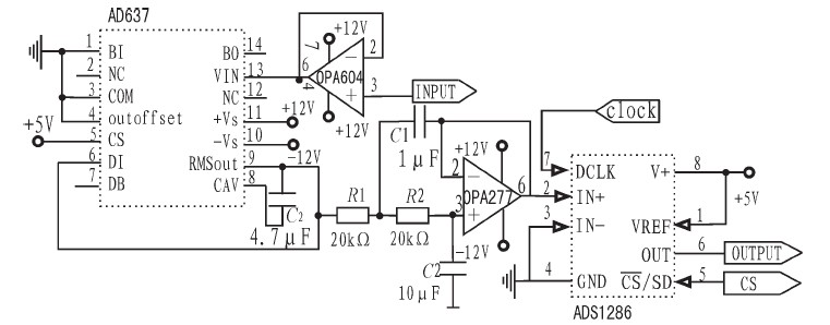
    The true RMS detection chip AD637 is used in the power measurement circuit to detect the true RMS of the signal, which is then sampled by the 12 bit serial interface and the 20 kHz sampling rate ad chip ads1286 and then sent to the FPGA for processing by the program to calculate the power and display it. As shown in Figure 6.
Fig. 6 power measurement and display circuit

     An emitter follower composed of opa604 has reached the function of isolating the front and rear stages. Changing the value of the average capacitance can set the average time constant and determine the low-frequency accuracy, the size of the output ripple and the stability time. The AC ripple component can be reduced by increasing the value of this capacitance, but this will increase the establishment time. Therefore, the method followed by a second-order active low-pass filter is selected to reduce the output ripple. After the true RMS is obtained, it is directly sent to ads1286 for analog-to-digital conversion, and then processed by FPGA to calculate the output power of the system and display it.

4 Design of system software
    According to the requirements of the topic, in order to realize the measurement and display function of the system power, the hardware adopts 8-bit CPU AT89S52, which is realized by C51 programming. The single chip microcomputer GUI should complete the functions of controlling ads1286, collecting data, calculating power and sending display. FPGA (ep1c6qc240 of cyclone series of ATERA company) is used as a bus controller to manage the data exchange between LCD and a / D and MCU. Using Verilog HDL language in quartus9 1 environment.
5 test methods and results

1    5 MHz function signal generator model: Agilent 33120A
    Digital oscilloscope model: Tektronix TDS 1002, dual channel, 60 MHz
    DC power model: sg173sb3, voltage and current stabilizing type
Four and a half digit multimeter model: fluke 45 dual display multimeter
5.2 test scheme and result analysis
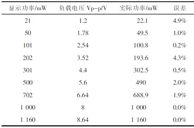
    1) The Agilent signal source is used to give the input audio signal for power display error measurement. The oscilloscope measures the voltage peak VO on the load at the single end output test point, calculates the actual power according to the formula, and then calculates the display error. The results are shown in Table 1.


    Table 1 test data of passband performance of amplification circuit

    It can be seen from the data in the table that the system power display module has 4-digit digital display, the accuracy is better than 5%, and the error is small.

    2) For noise, the Agilent signal source is used to give the input audio signal (ensure that the signal frequency is below 20 kHz), and 0.1 μ F capacitor for AC short circuit between input end and ground, and measure the noise at output end with oscilloscope. At this time, the measured noise is 2.96mv

    3) The efficiency measurement uses the DC power supply to supply power to the power amplifier circuit separately, so as to test the efficiency. The power supply voltage is + 5 v. the input signal is given in the same way as the passband. Observe the amplitude of the output signal with an oscilloscope, adjust the output to 200 MW and 500 MW, string the four and a half digit multimeter into the amplifier circuit, and measure the circuit current I. calculate the efficiency of the power amplifier according to the formula. The results are shown in Table 2.

    Table 2 efficiency test data of power amplifier circuit

    It can be seen from the table that when the output power is 500MW, the efficiency of the power amplification circuit is as high as 64.10%, which greatly meets the requirements of the subject; When the output is 200 MW, the efficiency also reaches 43.96% The system can realize high-efficiency audio amplification.

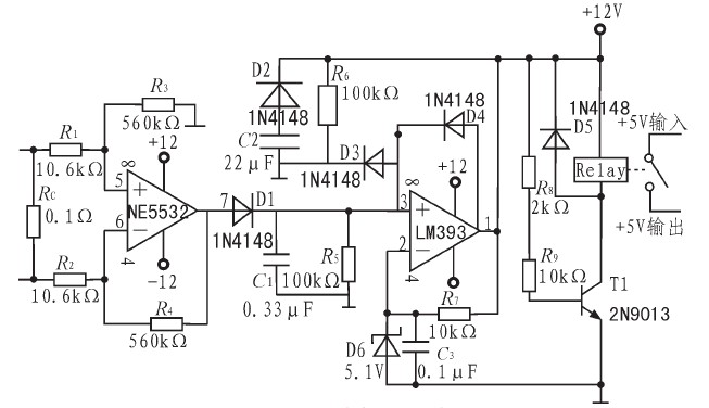
    4) The overcurrent protection measurement gives the input signal in the same way as the passband measurement. Observe the amplitude of the output signal with an oscilloscope and short circuit both ends of the load. It can be seen that the warning light of the short circuit module is on, the power supply of the power amplification part is cut off and the output becomes zero, so as to achieve the purpose of protection.

    6 Conclusion
    The system realizes the amplification and processing of audio signal, and completes the functions of high-efficiency power amplification, signal transformation, power measurement and display, overcurrent protection and so on. The system has good performance and high indexes in power and efficiency. Amplification circuit, signal transformation, power measurement and short-circuit protection have received good results. Especially in terms of power, it can reach 1.16 W, the efficiency can reach 64%, the noise is very low, and the display error of power measurement is small. Simple operation and flexible human-computer interaction.

    Disclaimer: This article is transferred from other platforms and does not represent the views and positions of this site. If there is infringement or objection, please contact us to delete. thank you!
    
  中恒科技ChipHomeTek

Back Top