"As mentioned in" current path of boost dc/dc converter ", there are two paths for circuit wiring in PCB layout of boost dc/dc converter, one is that it will flow through large current related to input and output, and the other is that it will only flow through small current used to realize control.
Wiring of feedback path
As mentioned in "current path of boost dc/dc converter", there are two paths for circuit wiring in the PCB layout of boost dc/dc converter, one will flow through the large current related to input and output, and the other will only flow through the small current used to realize control.
Generally, the path through which only a small amount of current flows is the path of the signal system. It includes the wiring of the feedback path that can feed back the output voltage to the FB (feedback) pin, and also includes (depending on the power IC) the wiring of the signal path to the enable and shutdown pins that control on/off.
When wiring the signal system, special attention should be paid to the wiring of the feedback path. The wiring of the feedback path is to feed back the output voltage from the output line to the FB pin to stabilize the output voltage. Since it is connected to the input of the error amplifier inside the IC through the voltage dividing resistor used to set the output voltage, it is a line with high impedance.
If the impedance of the line is high, it is easy to be disturbed by noise. If the wiring of the feedback path is disturbed by noise, the output voltage will produce error, which may lead to unstable operation.
Note the following points about routing the feedback path. The circuit diagram on the left is simply a circuit diagram showing the connection, and the circuit diagram on the right is a schematic diagram showing the positions and wiring corresponding to the four points of attention (a) to (d).
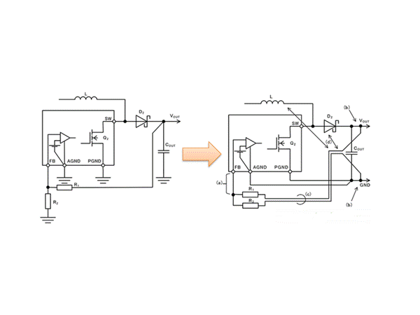
(a) The FB pin of the IC that inputs the feedback signal usually has a high impedance. The FB pin is connected with the resistive voltage dividing circuits of R1 and R2 through a short wire.
(b) The position for detecting the output voltage is connected to both ends of the output capacitor cout or behind the output capacitor.
(c) The wiring of resistance voltage divider circuit should be parallel and close to each other, so the noise resistance performance is better
(d) The wiring shall be away from inductance L and diode D2. Do not wire directly below the inductor and diode, and do not wire in parallel with the wiring of the power system. It is also applicable to multi-layer PCB.
Key points
In the PCB layout of boost dc/dc converter, the feedback path has high impedance and is easily disturbed by noise.
In the PCB layout of the boost dc/dc converter, if the wiring of the feedback path is disturbed by noise, the output voltage may cause error, or the operation may become unstable.
In the PCB layout of boost dc/dc converter, please pay attention to the four precautions in this article when routing the feedback path.

 Service mailbox
 13823783658
 ChatNow