
The formula is derived in continuous current mode, ignoring other parasitic resistances and diode on voltage drop, and the actual value is larger. If the inductance value is less than lmin, the inductance may be magnetically saturated, resulting in a great decline in the efficiency of the DC-DC circuit, or even the normal output of stable voltage.
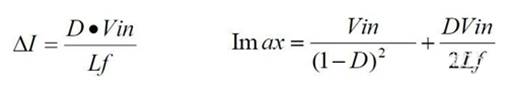
Second, considering the current ripple through the inductor, the parasitic parameters are also ignored in the continuous current mode,
When l is too small, the current ripple on the inductor will be too large, causing the maximum current passing through the inductor, Schottky diode and the power tube in the chip to be too large. Because the power transistor is not ideal, the power loss on the power transistor will increase at a particularly large current, resulting in the reduction of the conversion efficiency of the entire DC-DC circuit.
Third, generally speaking, when efficiency is not considered, the load capacity of small inductance is stronger than that of large inductance. However, under the same load conditions, the current ripple and maximum current value of the large inductance are small, so the large inductance can make the circuit start at a lower input voltage (the above conclusions are derived under the same parasitic resistance conditions).
In order to reduce the size of the external inductance, the operating frequency can be increased. For example, if the operating frequency is 350khz, only an inductance of more than 3.3uh is required to ensure normal operation. However, if the output terminal needs to output a large current (for example, the output current is greater than 50mA), it is recommended to use a large inductance in order to improve the working efficiency.
Under large load, the series resistance of the inductor will greatly affect the conversion efficiency. Assuming that the resistance of the inductor is RL and the load resistance is rload, the power loss of the inductor is roughly calculated as follows:
After comprehensive consideration, it is recommended to use 27uh
2. Output capacitance selection
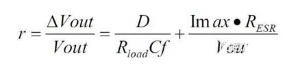
Output capacitors reduce load ripple and help provide a stable output voltage during load transients. When considering the ESR of the capacitor, the ripple of the output voltage is:
In order to reduce the output ripple, a large output capacitance is required. However, if the output capacitance is too large, the reaction time of the system will be too slow. Therefore, 100uF capacitor is recommended. If a smaller ripple is required, a larger capacitance is required.
When the output is connected to a large load, the ripple caused by ESR will become the most important factor. At the same time, ESR will increase efficiency loss and reduce conversion efficiency. Therefore, it is recommended to use tantalum capacitors with low ESR, or multiple or X7R ceramic capacitors in parallel. Other types of capacitors may have higher ESR, which will reduce the efficiency of the converter.
3. Diode
Rectifier diodes have a great impact on DC-DC efficiency. Although common diodes can make DC-DC circuits work normally, they will reduce the efficiency by 5~10%. Therefore, it is recommended to use Schottky diodes with low forward conduction voltage and short reaction time, such as 1N5817, 1N5819, 1N5821, 1N5822, etc.
In terms of specific parameters, the average forward rated current of the diode must be equal to or higher than the maximum output current, the repetitive peak forward rated current must be equal to or higher than the peak current of the inductor, and the reverse breakdown voltage must be higher than the rated voltage of the internal power switch.
For example, mcp1665 has an internal switch of 36V, which can provide up to 1A current. Therefore, microchip recommends using stps2l40vu Schottky diode supplied by STMicroelectronics. The reverse breakdown voltage of this device is 40V and the forward current is 2A.
4. Input capacitance
If the input power supply is stable, the DC-DC circuit can output low ripple and low noise current and voltage even if there is no input filter capacitor. However, when the power supply is far from the DC-DC circuit, it is recommended to add a filter capacitor of more than 10uF at the input of the DC-DC to reduce the output noise.
The DC-DC boost voltage regulator has high-speed switching characteristics and is very sensitive to PCB layout: parasitic inductance and capacitance may lead to high output ripple, poor output voltage stabilization effect, excessive electromagnetic interference (EMI), and even failure due to high voltage spikes. Therefore, the peripheral components should be close to the IC chip, and the grounding node should be close to the IC power grounding pin to minimize the loop area. The power grounding, signal grounding and heat conduction pad should also be connected together at a single low impedance grounding point.
|
Disclaimer: This article is transferred from other platforms and does not represent the views and positions of this site. If there is infringement or objection, please contact us to delete. thank you!
中恒科技ChipHomeTek
|
.jpg)


 Service mailbox
 13823783658
 ChatNow