MOSFET used as power switch
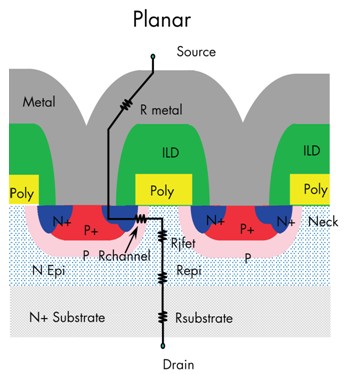
With the continuous optimization of device design for decades, power MOSFET transistors have brought new circuit topology and improved power efficiency. Power devices have changed from current driven to voltage driven, accelerating the market penetration of these products. In the 1980s, the planar gate power MOSFET was first oriented to high-voltage devices, and the bvdss voltage range reached 500-600v, making it a success in the market. During this period, the conduction loss of power MOSFET mainly depends on channel density, junction field effect transistor (JFET) impedance and epitaxial impedance (see Figure 1). With the more and more sophisticated lithography equipment in the semiconductor industry, the transistor cell density is increased and the conduction loss is improved. The lithography equipment can achieve higher cell density, and at the same time, the bvdss range of power MOSFET is successfully reduced to less than 100V, realizing new automotive electronics, power supply and motor control applications. The conduction loss of high voltage MOSFET is transferred to epitaxial design. On the other hand, the use of MOSFET devices in step-down converters and the requirement for a wider supply voltage range (30V) have stimulated the market demand for higher performance devices.
Figure 1: on impedance element of planar power MOSFET
With the rapid development of planar power MOSFET technology in the early 1990s, a new type of channel gate power MOSFET emerged, setting a new performance benchmark for low-voltage devices. This kind of Channel MOSFET adopts a gate structure embedded in the channel region and carefully etched into the device, doubling the channel density (the first generation products reached 12million cells per square inch). Since the new technology can increase the number of parallel conduction channels and reduce JFET impedance components, the conduction efficiency is increased by nearly 30%.
The challenge for device designers is: in addition to increasing the cell density, the technology improvement will increase the capacitive reactance and grid charge at the same time because the grid drain area and the grid source area increase. Therefore, device designers always hope to reduce switching losses through structural innovation. Fairchild Semiconductor introduced a channel gate power MOSFET optimized for high-efficiency buck converters in 1998, that is, the first generation powertrench ® Products. Today powertrench ® It has been optimized for seven generations and evolved into the latest buck converter components.
Power MOSFET optimization for synchronous rectifier topology
As the first batch of microcontrollers began to use standard 5V or 12V power supplies different from computers, power MOSFETs also began to be widely used. The old buck converter, which converts DC voltage into lower voltage, has become the application driving force for the development of low-voltage switching power devices. Moreover, the development focus has shifted from AC-DC switching power supply and motor drive to more demanding processors and related peripheral components that can meet specific power supply requirements.
As the power supply of the processor, the step-down converter is then equipped with synchronous rectifier to improve efficiency, and uses synchronous switching power MOSFET to supplement and eventually replace Schottky rectifier diode, so as to reduce conduction loss. The emergence of mobile computing technology has put forward higher requirements for converter efficiency, which has promoted the high evolution of this technology and become the mode used in modern power MOSFET.
At the high technology level, it is easy to determine the requirements for step-down converter MOSFET. In most cases, synchronous rectifier or syncfet ™ Both of them work in the on state, and their on impedance should be very small to minimize power consumption. The high side switch MOSFET is driven by the DC power supply to generate electrical pulses, which are smoothed into continuous voltages by the LC filter, and then applied to the load. Because the main loss of MOSFET comes from the switching action and the conduction time is very short, the switching device should be fast enough and the conduction impedance should be small enough. The two links of switch and rectifier are alternately in the conduction state, but the conduction period cannot overlap, otherwise the so-called shoot through will be formed between the power supply and grounding, directly causing power loss. When the switching device is on, the syncfet ™ The magnitude of the induced current and voltage on the grid CGS will depend on the amplitude and ratio of CGS and CGD and the switching transient rate. If the gate voltage exceeds the threshold, the device will turn on again, resulting in a straight through. Therefore, as long as the cgs/cgd ratio is large enough, it can prevent drain voltage transients from inducing through.
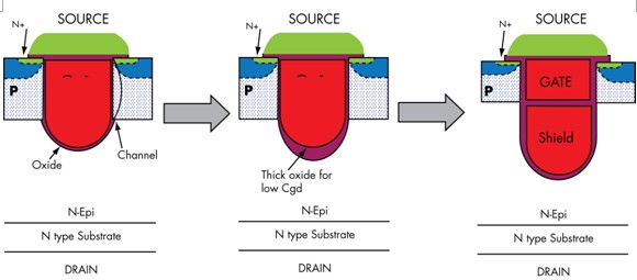
After analyzing the technology evolution and defining the requirements of MOSFET, we can understand the main driving factors of device technology development. In the basic channel gate structure of Fig. 2a, the on impedance can be reduced by increasing the width / length ratio of the channel. Extending the oxide layer thickness at the bottom of the channel as shown in Figure 2B can improve the switching speed and increase the cgs/ CGD ratio. The final setting is as shown in Fig. 2C. An additional electrode is embedded in the lower part of the gate of the channel to increase the charge in the drift region, thereby reducing the on impedance; At the same time, the CGD is reduced, the switching speed is increased, and the CGS /cgd ratio is changed, so as to prevent straight through to the greatest extent.
Figure 2:a) conventional channel gate power MOSFET; b) Channel MOSFET with thickened oxide layer at the bottom of the channel; c) Channel MOSFET with shield electrode added.
In the past several generations of devices, it is necessary to integrate a Schottky diode in the low side synchronous rectifier to reduce the dead time conduction loss of MOSFET body diode and control the voltage transient generated when the body diode recovers in reverse. In order to eliminate the relatively high cost Schottky diodes, the latest generation of products adopt diode forward injection to minimize the drain shielding capacitive reactance, reduce the shielding impedance and other professional technologies, and strive to suppress those adverse voltage transients, such as drain voltage overshoot.
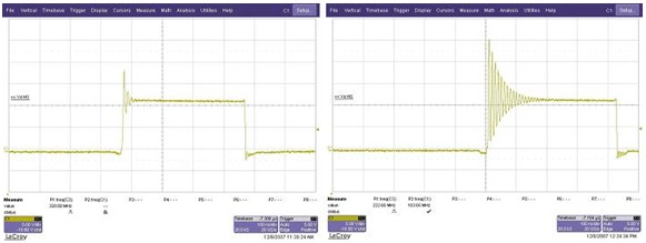
As shown in figures 3a and 3b, the voltage overshoot and oscillation of the new product are even much lower than those of devices with integrated Schottky components. The drain voltage oscillation of syncfet is damped and suppressed, which greatly reduces the EMI noise common in such applications. The solution has extremely quiet switching characteristics and can completely eliminate the external buffer circuit used to eliminate oscillation
3: Comparison between quiet switching behavior (a) and traditional channel product switching behavior (b)
Due to the continuous evolution of device technology, new products have begun to blossom. These products improve the performance and the maximum output current of voltage converters by reducing the power consumption of MOSFET switches. At present, syncfet usually uses three milliohm components, so that the output current of each stage of polyphase converter can reach more than 30A. This is a remarkable achievement in comparison to the packaging interconnection impedance between components of past generations of products, which is close to the overall impedance of today‘s powertrench products. The package interconnection impedance is reduced by eight times, which makes a quadruple improvement on the semiconductor impedance in the past 10 years. As a result, the output current of the converter is doubled. The development of new products in the future also includes increasing the operating frequency, making the filter inductance and capacitance smaller, thus reducing the space of the circuit board used.
Multichip modules containing encapsulated controllers and / or drive circuits and power switches are entering the consumer electronics market, such as game consoles and portable computers. The advantages of these new components include reducing the parasitic inductance factor of the circuit board, avoiding the voltage transients generated by the discrete component scheme, and the inherent weakness of depriving power from the converter, so as to prolong the battery life, reduce the operating temperature, reduce the radiated noise or EMI, and reduce the circuit board size.
Most of the progress in packaging and MOSFET device technology comes from the increasing use of simulation technology, which enables engineers to develop innovative solutions. The development of semiconductor technology described in this paper depends on the finite element simulation analysis of devices and the simulation analysis of applications, so as to have a deeper understanding of the interaction among semiconductor, packaging, gate drive circuit and circuit board parasitic factors. Simulation technology can also make people deeply understand the process links of device parameter changes, and find solutions to eliminate these changes to the greatest extent.
conclusion
To develop advanced power devices for advanced power supplies and achieve good market results, we must consider and adapt to the evolving application needs. This requires a lot of optimization work for all components in the application, including the semiconductor chip, packaging, circuit board layout of power devices, and the operating frequency of the converter. Fairchild Semiconductor recognizes this challenge and uses new design principles to develop power MOSFETs. Fairchild Semiconductor has professional advantages in power design, which makes its powertrench product functions take a leading position in the industry.
|
Disclaimer: This article is transferred from other platforms and does not represent the views and positions of this site. If there is infringement or objection, please contact us to delete. thank you!
中恒科技ChipHomeTek
|

 Service mailbox
 13823783658
 ChatNow