Figure 1 Standard high precision
For accuracy, the amplifier of Figure 1 has an ultra-low input bias current and offset voltage. In order to reduce the current error by being lower than the minimum I PD, the max9613 has a rated input bias current of 1pA (typical). In order to maintain the linearity of photodiode response as much as possible, the max9613 offset voltage is 150mV (maximum) ultra-low.
This TIA may be unstable due to the surrounding actual capacitance and parasitic capacitance. But I hope that with the new design expertise you gain from this blog series, you will be able to design this unpleasant situation.
In Figure 1, the signal gain is equal to the combination of the feedback network and the parasitic resistance of the photodiode. The signal gain formula (formula 1) is:
V OUT / I PD ≈ (R F || C F ) 1
In equation 1, if C f is assumed to be an open circuit, the estimated DC gain of the transimpedance circuit is r F.
A further examination of equation 1 shows that the pole frequency (equation 2) is equal to:
ƒ P = 1 / (2 P R F X C f) equation. two
The signal frequency response shows a higher frequency DC response at RF and FP (Fig. 2).
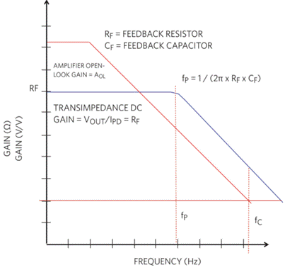
Figure 2 TIA signal frequency response.
In Fig. 2, the signal is obtained on the inverting side of the amplifier. The DC gain of TIA is equal to V out /i PD. Conveniently, this gain is equal to the feedback resistance R F. As the frequency increases, the gain remains stable until the corner frequency is reached, where R F and C f form a low-pass filter.
This is the story of TIA signal response, but we haven‘t talked about stability or circuit ringing in the AC domain. Figure 1 has two basic areas that we will use to further illustrate the AC stability response:
1) Op amp circuit, which will include all op amp parasitic effects.
2) Photodiode with all photodiode parasitic effects.
The element and parasitic capacitance and resistance in these two regions will constitute the step response characteristics. In our upcoming evaluation, we will understand how the parasitic capacitance of the amplifier and photodiode has a significant impact on the stability of the circuit.

 Service mailbox
 13823783658
 ChatNow