Charging pump (non inductive) dc/dc converter is popular in space limited applications. It must be powered by low to medium load current. This kind of converter adopts a small package, which has low static working current and requires the least external components. However, noise generation is a less desirable feature of many charging pumps.
These unwanted noises can cause many problems. In wireless applications, the noise generated by power input will interfere with RF transmission and reception, while the noise at output will be coupled with those sensitive circuits, and even produce audible noise. The new ltc3200 series booster charging pump adopts a new structure, which can minimize the input and output noise to avoid the above unwanted interference.
Burst Mode ® Burst mode and constant frequency
Most adjustable charging pump dc/dc converters adopt burst mode burst mode architecture. Although this regulator structure has the lowest static current, it also produces the largest input and output noise. For devices with burst mode, the charging pump switch provides the maximum current to the output, or it is completely turned off. In order to adjust the output, the hysteresis comparator and benchmark control the on and off of the charging pump. When there is low-frequency ripple at the output, it needs to be adjusted (as shown in Figure 1). This one on one off burst will lead to a large input ripple current, so it must be powered by the input power supply. Any impedance in the input power supply will produce voltage noise at the input end, which must be eliminated by other circuits powered by the same power supply.
Table 1: typical burst mode output ripple.
Ltc3200 and ltc3200-5 charging pumps have been designed to minimize input and output noise. These devices are adjustable booster charging pumps that can provide output current of up to 100mA. Ltc3200-5 can provide stable 5V output voltage and is packaged with 6-pin SOT-23; The ltc3200 can generate adjustable output voltage and is packaged with 8-pin MSOP.
Both devices adopt constant frequency architecture to reduce low-frequency output noise. Even if there is no load, the switch of the charging pump is continuous. The linear control loop is responsible for regulating the total amount of charge transmitted to the output in each clock cycle. Since the output regulation loop is linear, the peak to peak output ripple is approximately vripple = (iload/cout) / (2 • FOSC), and no additional ripple is generated due to the hysteresis of the regulator.
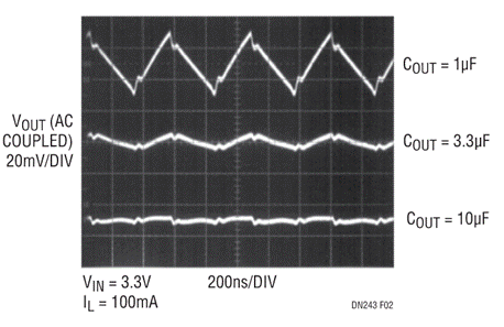
Even if a small output capacitor is used, the 2MHz oscillation frequency of the device can also allow low output ripple. Figure 2 shows the output ripple of ltc3200-5 when the output capacitor with different values supports 100mA load current.
Figure 2: output ripple of ltc3200-5.
Reduce input noise
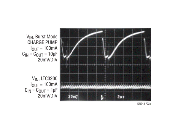
Although a single constant frequency can improve the input noise, the ltc3200 series also takes a step forward. It uses a unique built-in control circuit to adjust the input current of the charging pump under two clock phases. This technology can prevent the RC current from attenuating in one or two half clock cycles of the charging pump oscillator, which minimizes the reference input ripple by changing the input current. Figure 3 shows the input noise difference between ltc3200 and typical burst mode charging pump. As shown in the figure, both devices can obtain an output current of 100mA and a stable output voltage of 5V from an input voltage of 3.6V. The input impedance of 0.1 Ω is used for testing. The typical burst mode charging pump device adopts 10 at both input and output μ F ceramic capacitor, ltc3200 adopts 1 with the same dielectric μ F ceramic capacitor. As shown in Figure 3, even if the bypass capacitance is reduced to 1/10, the input noise can be significantly reduced by using ltc3200.
Figure 3: input noise test circuit.
Typical applications
Charging pumps usually provide low-power boost conversion for handheld electronic devices such as mobile phones and PDAs. These devices, especially those containing RF communication circuits, are very sensitive to noise. A popular application of low-noise charging pumps is to power white LEDs to provide backlight for small color LCD displays. The circuit shown in Figure 4 is a low-noise boost power supply, which can drive up to 6 white LEDs. The FB pin of ltc3200 is used to adjust the LED current flowing through each LED ballast. With ltc3200, users can directly use the battery to provide boost power for the backlight circuit, eliminating the clumsy problem of low-frequency noise filtering.
|
Disclaimer: This article is transferred from other platforms and does not represent the views and positions of this site. If there is infringement or objection, please contact us to delete. thank you!
中恒科技ChipHomeTek
|


 Service mailbox
 13823783658
 ChatNow