Key points of this paper:
Since the pin assignment of the to-247-4l package with driver source pins and the to-247n package without driver source pins are different, attention should be paid to the pattern layout.
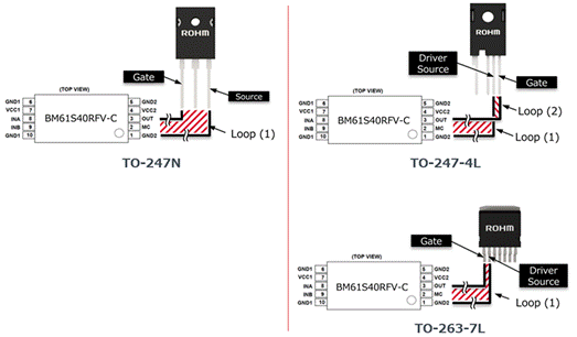
When to-247-4l is connected to the gate driver, due to the pin allocation, the wiring must cross and they cannot be arranged on the same plane. Therefore, the out signal and the gnd2 signal will form two loops, and a surge will occur according to the loop area and its ratio.
As a countermeasure, it is necessary to reduce the area of the loop as much as possible and make the areas of the loop (1) and the loop (2) equal. In addition, it is also necessary to consider adding a basic surge suppression circuit or even a buffer circuit.
In this article, we will discuss the considerations related to the circuit board layout and wiring of the to-247-4l package product with driver source pins. Because the pin allocation of the to-247-4l is different from that of the traditional package, it is necessary to pay attention to the layout and wiring.
Circuit board layout and wiring considerations for to-247-4l with driver source pins
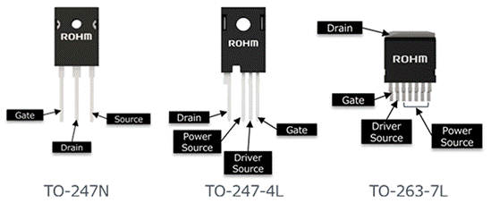
As described in the article "package with driver source pins", the pin allocation of to-247-4l with driver source pins is different from the traditional to-247n. Here again, the pin distribution diagrams of the conventional to-247n, to-247-4l with driver source pins and to-263-7l are given.
The gate pin of the to-247-4l is located on the right most side facing the mark surface, while the gate pin of the conventional to-247n package is located on the left most side. MOSFETs are usually driven by driver ICs, but the pin allocation of most driver ICs is suitable for the traditional to-247n package. The following is an example of MOSFET wiring diagram when Rohm driver IC bm61s40rfv-c is used.
In the case of to-247n, the driving signal out and the return signal gnd2 of the MOSFET are arranged in the same order as the gate pin and the source pin, so the lines can be routed in parallel on the same plane.
In the to-247-4l package, the arrangement of the gate pin and the driver source pin is opposite to that of the driver IC. As shown in the figure, the wiring must cross and cannot be arranged on the same plane. Therefore, as shown in the figure, the out signal and the gnd2 signal form two loops, and attention should be paid to the area ratio of the loop areas (1) and (2).
In general, MOSFETs in the to-247-4l package are used in environments where the D / dt value is large. When the magnetic flux changes (D Φ/ DT) is orthogonal to the loop area, an electromotive force proportional to the loop area of the drive circuit is generated. Moreover, under certain loop area ratios between the gate and the source of the MOSFET, the voltage value may sometimes reach a level that may cause problems such as positive surges and negative surges. Therefore, it is necessary to make the loop area formed by the out signal and the gnd2 signal as small as possible, and make the areas of the loop (1) and the loop (2) equal.
The pin distribution of the to-263-7l package is the same as that of the to-247n, so two loops like that of the to-247-4l cannot be formed. Therefore, the same method as the traditional method can be used for wiring. However, since the driving IC of Rohm is provided with gnd2 pins on both sides (pin 1 and pin 5) of the driving signal out pin, even the to-247-4l package can be wired using the same method as the conventional package.
In addition, in some previous articles, it was suggested to increase the VGS surge suppression circuit, but even so, the VGS surge may still exceed the VGS rated value due to the ringing when the VDS is turned off. In this case, the VGS surge can be suppressed within the rated range by reducing the wiring impedance from the HVDC or adding a buffer circuit to each MOSFET. For how to design the buffer circuit, please refer to the application guide "design method of buffer circuit".
|
Disclaimer: This article is transferred from other platforms and does not represent the views and positions of this site. If there is infringement or objection, please contact us to del
中恒科技ChipHomeTek
|

 Service mailbox
 13823783658
 ChatNow