Continuous sine wave and music
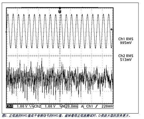
When evaluating the performance of class D amplifier in the laboratory, continuous sine wave is often used as the signal source. Although it is convenient to use sine wave for measurement, the result of such measurement is the thermal load of the amplifier in the worst case. If a class D amplifier is driven with a continuous sine wave close to the maximum output power, the amplifier often enters a thermal off state.
The RMS value of common sound sources, including music and speech, is often much lower than the peak output power. Typically, the peak to RMS power ratio (i.e., peak factor) of speech is 12 dB, while the peak factor of music is 18 dB to 20 dB. Fig. 1 shows the waveform diagram of audio signal and sine wave in time domain, and gives the results of RMS values measured by oscilloscope. Although the peak value of the audio signal is slightly higher than that of the sine wave, its RMS value is only about half of that of the sine wave. Similarly, there may be abrupt changes in the audio signal, but as shown by the measurement results, the average value is still far lower than the sine wave. Although the audio signal may have a peak value similar to that of the sine wave, the thermal effect of the class D amplifier is much lower than that of the sine wave. Therefore, when measuring the thermal performance of the system, it is better to use the actual audio signal rather than the sine wave as the signal source. If only sine wave is used, the thermal performance obtained is worse than that of the actual system.
Precautions for PCB heat dissipation
In the industrial standard TQFN package, the exposed pad is the main way of IC heat dissipation. For packages with bare pads at the bottom, the PCB and its copper layer are the main heat dissipation channels of class D amplifiers. As shown in Fig. 2, it is best to solder the bare pad to the large-area copper block according to the following principles when attaching the class D amplifier to the common PCB. As far as possible, lay more copper clad between the copper clad block and the adjacent class D amplifier pins with equal potential and other elements. In this case, the copper layer is connected to the upper right and lower right of the heat dissipation pad (as shown in Fig. 2). The copper wiring shall be as wide as possible because it will affect the overall heat dissipation performance of the system.

The copper block connected with the bare pad should be connected to other copper blocks on the back of the PCB through multiple vias. The copper block shall have as large an area as possible under the condition that it meets the requirements of system signal wiring.
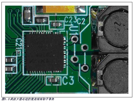
Try to widen all connections with devices, which will help improve the heat dissipation performance of the system. Although the pin of the IC is not the main heat dissipation channel, there is still a small amount of heat generation in practical applications. In the PCB shown in Fig. 3, the output of the Class-D amplifier is connected to the two inductors on the right side of the figure by wide wires. In this case, the copper core winding of the inductor can also provide an additional heat dissipation channel for the D amplifier. Although the overall thermal performance is improved by less than 10%, such improvement will bring two different results to the system - even if the system has better heat dissipation or serious heat generation.
Auxiliary heat dissipation
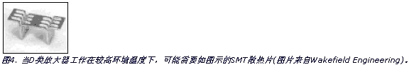
When the Class-D amplifier operates at a high ambient temperature, adding an external heat sink can improve the thermal performance of the PCB. The thermal resistance of the heat sink must be as small as possible to optimize the heat dissipation performance. After using the bare pad at the bottom, the bottom of PCB is often the heat dissipation channel with the lowest thermal resistance. The top of the IC is not the main heat dissipation channel of the device, so it is not cost-effective to install the heat sink here. Figure 4 shows a PCB surface mounted heat sink (218 series, provided by Wakefield Engineering). The heat sink is welded on the PCB, which is an ideal choice for taking into account the size, cost, assembly convenience and heat dissipation performance.
Thermal calculation
The die temperature of class D amplifier can be estimated by some basic calculations. In this example, the temperature is calculated according to the following conditions:
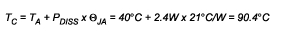
AM=+40℃
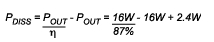
POUT=16W
Efficiency( η)= 87%
θ JA=21℃/W
First, calculate the power consumption of class D amplifier:
Then, the die temperature TC is calculated by power consumption, and the formula is as follows:
According to these data, it can be inferred that the device has ideal performance when it works. Because the system can rarely work at the ideal ambient temperature of 25 ℃, it should be reasonably estimated according to the actual operating ambient temperature of the system.
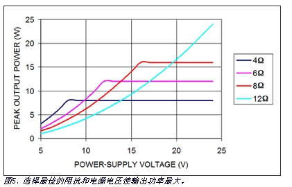
Load impedance
The on resistance of MOSFET output stage of class D amplifier will affect its efficiency and peak current capability. Reducing the peak current of the load can reduce the I2R loss of the MOSFET, thereby improving the efficiency. To reduce the peak current, the speaker with the maximum impedance shall be selected under the conditions of ensuring the output power, the voltage swing of the class D amplifier and the limitation of the power supply voltage, as shown in Fig. 5. In this example, it is assumed that the output current of the class D amplifier is 2a and the power supply voltage range is 5V to 24V. When the power supply voltage is greater than or equal to 8V, the load current of 4 Ω will reach 2a, and the corresponding maximum continuous output power is 8W. If the output power of 8W can meet the requirements, a 12 Ω speaker and 15V power supply voltage can be considered. At this time, the peak current is limited to 1.25A, and the corresponding maximum continuous output power is 9.4w. In addition, the working efficiency of 12 Ω load is 10% to 15% higher than that of 4 Ω load, reducing power consumption. The actual efficiency improvement varies according to different class D amplifiers. Although the impedance of most speakers is 4 Ω or 8 Ω, other impedance speakers can also be used to achieve more efficient heat dissipation.
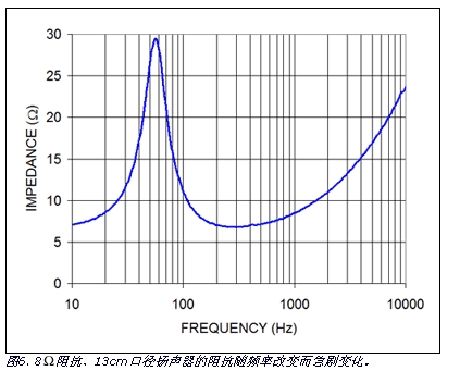
In addition, it is also necessary to pay attention to the change of load impedance within the audio bandwidth. Loudspeaker is a complex electromechanical system with many resonant elements. In other words, an 8 Ω speaker exhibits an 8 Ω impedance only in a very narrow frequency band. In most audio bandwidth, the impedance will be greater than its nominal value, as shown in Figure 6. In most audio bandwidth, the impedance of the speaker will be much greater than its nominal value of 8 Ω. However, the presence of tweeters and frequency dividing networks will reduce the impedance value. Therefore, the total impedance of the system must be considered to ensure sufficient current driving capability and heat dissipation performance.
conclusion
The efficiency of class D amplifier is much higher than that of class AB amplifier. Although this efficiency advantage reduces the requirements of system design for heat dissipation performance, the heat dissipation of the system can not be completely ignored. However, if we can follow good design principles and set reasonable design goals, using class D amplifiers can make the audio system design simpler.
|
Disclaimer: This article is transferred from other platforms and does not represent the views and positions of this site. If there is infringement or objection, please contact us to del
中恒科技ChipHomeTek
|

 Service mailbox
 13823783658
 ChatNow