When designing ADC circuit, a common problem is "how to protect ADC input under overvoltage", then
What problems may occur in the case of overvoltage?
How often does it happen?
Is there any potential remedy?
For the above problems, let‘s conduct an in-depth analysis!
Overdrive of ADC input generally occurs when the rail of the drive amplifier is far greater than the maximum input range of ADC. For example, the amplifier uses ± 15 V for power supply, while the ADC input is 0 to 5 V. High voltage rail is used to accept ± 10 V input and supply power to ADC front-end signal conditioning/drive level, which is very common in industrial design, such as PLC module. If a fault condition occurs on the drive amplifier rail, the ADC may be damaged by exceeding the maximum rating, or the synchronization/subsequent conversion may be disturbed in a multi ADC system.
Although the focus discussed here is how to protect precision SAR ADC, such as AD798x series, these protective measures are also applicable to other ADC types~
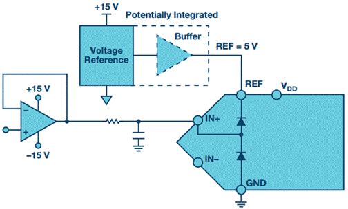
Consider the situation in Figure 1.
Figure 1. Typical circuit diagram of precision ADC design
The circuit above represents the AD798X (such as AD7980) series PulSAR ® Circumstances in ADC. There is a protective diode between the input, the reference voltage source and the ground. These diodes can handle large currents up to 130mA, but can only last for a few milliseconds, and are not suitable for long periods of time or repeated overvoltage. On some products, such as AD768X/AD769x (such as AD7685 and AD7691) series devices, the protective diode is connected to the VDD pin instead of REF. On these devices, the VDD voltage is always greater than or equal to REF. In general, this configuration is more effective because VDD is a more stable clamping rail and is not sensitive to interference.
In Figure 1, if the amplifier tends to+15 V rail, the protection diode connected to REF will turn on and the amplifier will attempt to pull up the REF node. If the REF node is not driven by the strong driver circuit, the voltage of the REF node (and input) will rise above the absolute maximum rated voltage. Once the voltage exceeds the breakdown voltage of the device in this process, ADC may be damaged. Figure 3 illustrates the case where the ADC driver tends to 8 V and drives the reference voltage (5 V) over. Many precision reference voltage sources have no current filling capacity, which will cause problems in this case. Or, the reference driver circuit is strong enough to keep the reference voltage near the nominal value, but it will still deviate from the precise value.
In a synchronous sampling multi ADC system sharing a reference voltage source, the conversion on other ADCs is not accurate because the system depends on a highly accurate reference voltage. If the fault recovery time is long, the subsequent conversion may also be inaccurate.
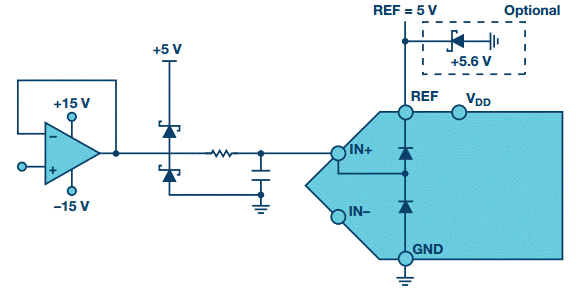
There are several different ways to alleviate this problem. The most common is to use Schottky diodes (BAT54 series) to clamp the amplifier output in the ADC range. See Figures 2 and 3 for details. If applicable, diodes can also be used to clamp the input to the amplifier.
Figure 2. Typical circuit diagram of precision ADC design
(Schottky diode and Zener diode protection are added)
In this case, the Schottky diode is selected because it has a low positive conduction voltage drop and can be turned on before the internal protection diode in the ADC. If the internal diode is partially turned on, the series resistance behind the Schottky diode also helps to limit the current within the ADC. For additional protection, if the reference voltage source has no/almost no current sinking capability, zener diodes or clamping circuits can be used on the reference node to ensure that the reference voltage is not excessively pulled up. In Figure 2, a 5.6V Zener diode is used for a 5V reference voltage source.
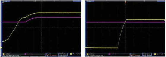
Figure 3. Yellow=ADC input,
Purple=reference voltage source.
Schottky diode is not added to the left image,
Schottky diode is added to the right image
Figure 3. Yellow=ADC input,
Purple=reference voltage source.
Schottky diode is not added to the left image,
Schottky diode is added to the right image
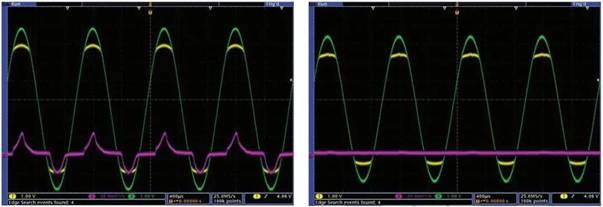
The example in Figure 4 shows the impact on the reference input (5V) after adding a Schottky diode to the ADC input when the ADC input is overdriven by a sine wave. Schottky diode is grounded, and 5 V system rail can absorb current. If there is no Schottky diode, when the input voltage exceeds a voltage drop of reference voltage and ground voltage, reference voltage source interference will occur. It can be seen from the figure that the Schottky diode completely eliminates the reference voltage source interference.
Attention should be paid to the reverse leakage current of Schottky diodes, which can introduce distortion and nonlinearity during normal operation. This reverse leakage current is greatly affected by temperature and is generally specified in the diode data manual. BAT54 series Schottky diode is a good choice (maximum value is 2 at 25 ° C μ A. Approx. 100 at 125 ° C μ A)。
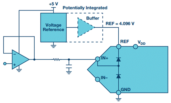
One way to completely eliminate the overvoltage problem is to use a single power rail for the amplifier. This means that as long as the same power level (5V in this example) is used for the reference voltage (maximum input voltage), the drive amplifier will never swing below the ground voltage or above the maximum input voltage. If the reference circuit has sufficient output current and drive strength, it can be directly used to power the amplifier. Another possibility, shown in Figure 5, is to use a slightly lower reference voltage value (for example, 4.096 V when using a 5 V rail), which significantly reduces the voltage overdrive capability.
Figure 5. Typical circuit diagram of single power supply precision ADV design
These methods can solve the problem of input overdrive at the cost of limited input swing and range of ADC, because the amplifier has upper margin and lower margin requirements. Generally, the rail to rail output amplifier can be within more than 10 mV of the rail, but the input margin requirements must also be considered, which may be 1 V or higher, which will further limit the swing within the buffer and unit gain configuration. This method provides the simplest solution because no additional protective elements are required, but depending on the correct supply voltage, rail to rail input/output (RRIO) amplifiers may also be required.
The series R in the RC filter between the amplifier and the ADC input can also be used to limit the current at the ADC input during overvoltage conditions. However, when using this method, it is necessary to make a choice between the current limiting capacity and ADC performance. A larger series R provides better input protection, but will cause a greater distortion in ADC performance. If the input signal bandwidth is low, or ADC does not operate at full throughput rate, this trade-off is feasible, because series R is acceptable in this case. The acceptable R size for application can be determined experimentally.
As mentioned above, there is no way to protect the ADC input, but depending on the application requirements, different individual or combined methods can be used to provide the required level of protection with corresponding performance trade-offs.
|
Disclaimer: This article is transferred from other platforms and does not represent the views and positions of this site. If there is any infringement or objection, please contact us to delete it. thank you!
中恒科技ChipHomeTek
|

 Service mailbox
 13823783658
 ChatNow