ADI LT8618 (a 100mA high-speed synchronous monolithic step-down switching regulator) can expand the input range to 65V and the load capacity to 15mA. When the transmitter is packaged and exposed to harsh environmental changes, its high efficiency eliminates the thermal constraints in the current loop system design. It is recommended to use a low-cost filter to reduce voltage ripple and current ripple on the cable side. This paper analyzes the performance of the power regulator, and provides a guide for component selection to meet strict industrial requirements. In addition, test data such as efficiency, startup and ripple are also provided.
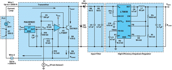
LT8618 is a compact buck converter with many functions, which can meet the requirements of industrial, automotive and other unpredictable power environment. It is ideal for 4mA to 20mA current loop applications, with ultra-low quiescent current, high efficiency, wide input range, up to 65V voltage and compact size. Figure 2 shows a complete transmitter circuit solution that uses the LT8618 to power the MAX6192C high-precision voltage reference, voltage current conversion, and other circuits.
Figure 2. Current loop with LT8618 as DC power supply
The current of the shunt circuit 2SC1623 is proportional to the voltage applied at the positive input of the error amplifier (EA). The 2.5V reference voltage is generated by MAX6192C. MAX6192C is a precise voltage reference IC with low noise, low voltage drop and low temperature drift of maximum 5ppm/° C. For intelligent sensors whose digital output is proportional to the environment variable, DAC can convert the digital signal into an analog signal and send it to the error amplifier.

Therefore, through EA, BJT (2SC1623) and 100 Ω (± 0.1%) detection resistance (RSENSE), the converter can modulate the current in the current loop from 4mA to 20mA, where 4mA represents non-zero minimum output and 20mA represents maximum signal. Even if the field transmitter has no process signal output, a non-zero minimum output of 4mA or an output above zero can also supply power to the equipment. Therefore, the current in the shunt circuit is proportional to environmental variables, such as pressure, temperature, liquid level, flow, humidity, radiation, pH value or other process variables.
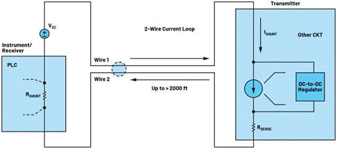
The two long wires are part of the information carrying current loop and are also used to supply power to the transmitter from the VDC (power supply on the receiver side). The minimum voltage of the VDC shall be sufficient to cover the voltage drop between the minimum operating voltage of the conductor, shunt and transmitter. The supply voltage depends on the application, usually 12V or 24V, but can also be as high as 36V.
At the remote transmitter terminal, Schottky diodes (D1) protect the transmitter from reverse currents. Placing a Zener diode or TVS (D2) diode at the input end can provide further protection, thereby limiting transient voltage surges that are proportional to the inductance of the current loop. The LT8618 high-efficiency monolithic step-down voltage regulator reduces the loop voltage to 5.5V or 3.3V to supply power to the reference, DAC and other functional units.
In Figure 2, the wiring between the VDC and the transmitter can range from a few feet to 2000 feet. The stray inductance of the current loop and the input capacitance of the step-down voltage regulator form an LC resonant slot. The power supply side (VDC) transient also occurs on the input side of the remote transmitter. For the worst case undamped oscillation, the peak voltage may be twice that of VDC. For example, if the typical value of the working input voltage is 24V and the maximum specification value is 36V, the maximum voltage on the transmitter side may exceed 65V. As shown in Figure 2, protection can be easily realized by using TVS diode D2 in front of the transmitter to limit any surge during the transient.
In addition, an efficient system can be built by using LDO regulators to protect the LT8618 from high voltage excursions. In this topology, the LDO regulator will adjust the input voltage minus its differential voltage, while the LT8618 will convert~24V to 5V or 3.3V with high efficiency. The current limiting value of LDO voltage regulator should be set below the normal 3.8mA, while maintaining high efficiency. The input capacitor of LT8618 will basically use decoupling capacitor and energy storage capacitor. This will enable high loads to break out at the back end for a short time with minimal or no current consumption of the current loop. As the high-voltage offset is relatively short, it usually carries less total energy, so during these transients, the power loss generated in the LDO regulator will not affect the overall efficiency; That is to say, the LDO regulator is almost always under a high voltage drop ratio.
A typical current loop will limit the input current of the power circuit supplying the entire remote transmitter, and the available load current of the LDO regulator cannot exceed this input current limit. On the other hand, the step-down voltage regulator can double the input current supplied to the load. Figure 3 shows the relationship between the output current and the input current of the LT8618 regulator when converting from 24V input voltage to 5.5V output. For the input current limiting value of 3.8mA, the output current is almost 15mA. This additional power can increase the operating margin and enable additional functional units, simplifying the work of system designers.
Figure 3. Relation between output current and input current, VIN=24V, VOUT=5.5V
Running in burst mode can improve the efficiency under light load
The efficiency of LDO regulator is proportional to the voltage drop ratio (VOUT/VIN). When the input voltage is slightly higher than the output voltage, the efficiency will be very high. Problems will occur when the pressure drop ratio is too high. At this time, the efficiency is very low, which will cause great thermal stress to the system. For example, when the input voltage is 55V and the output voltage is 3.3V, the power loss of the LDO regulator is 0.19W and the load current is 3.8mA. In contrast, a properly designed step-down regulator can be very efficient at high step-down ratio. In addition, compared with the asynchronous regulator, the synchronous step-down regulator can replace the freewheeling diode with MOSFET, thus improving the efficiency. The challenge for synchronous buck converter is to optimize the efficiency in the whole load range, especially in the light load of 3mA to 15mA, when the input voltage can be as high as 65V.
For a typical synchronous buck converter, there are three kinds of power losses: switching loss, gate drive loss and loss related to the logic circuit of the converter IC controller. If the switching frequency is reduced, the switching and gate drive losses can be greatly reduced. Therefore, as long as the converter is operated at low frequency, the switching and gate losses at light load can be reduced.
Under light load, the bias loss of logic circuit is equivalent to the relatively low switch related loss. The bias circuit is usually powered by the output, and only receives power from the input through the internal LDO regulator under startup and other transient conditions.
Under light load, the LT8618 operates in Burst Mode ®) To solve the logic circuit loss problem. At this time, the current is transmitted to the output capacitor in the form of short pulses, and then enters a relatively long sleep period, during which most logic control circuits are closed.
In order to improve the light load efficiency, larger inductance can be selected, because more energy can be transferred to the output during the short switching pulse, and the step-down regulator can also maintain the sleep mode for a longer time between these pulses. By prolonging the time between pulses as much as possible and minimizing the switching loss of each short pulse, the static current of the LT8618 can be lower than 2.5 μ A. At the same time, maintain the regulated output when the input voltage is up to 60V. Because the current of many transmitter circuits is relatively low most of the time, the current consumption is as high as tens or hundreds μ Compared with the typical step-down voltage regulator of A, this low quiescent current saves a lot of energy.
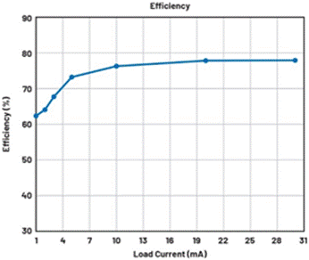
Figure 4 shows the efficiency of the current loop solution shown in Figure 2, where the 5.5VOUT output rail is connected to the BIAS pin of the LT8618. Under 100 mA full load, the peak efficiency reaches 87%, the input voltage is 28V, and the inductance is 82 µ H. Under the same 28V input voltage, the efficiency under 10mA load can reach or exceed 77%, showing outstanding performance.
Figure 4. High efficiency of LT8618 under light load, VIN=28V, VOUT=5.5V, L=82 µ H
Input filter for limiting impulse current and current loop ripple
The input of the power regulator is connected to the current loop. Therefore, in addition to steady state current limiting, it is also important to limit ripple current and surge current during startup or load transient. The impulse current during startup of power converter depends on the input capacitance and output capacitance in a given soft start time. This requires trade-offs: minimize the input capacitance to prevent the generation of large impulse current, while making it large enough to maintain an acceptable low ripple.
The input current of step-down converter is pulse current; Therefore, the input capacitor plays a key role in providing a filtering path for ripple current. Without this capacitor, a large amount of ripple current will flow through a long current loop, resulting in unpredictable voltage drop behavior. Therefore, there should be a minimum input capacitor that can meet the requirements of ripple current and ripple voltage. Multilayer ceramic capacitors (MLCC) have excellent performance in ripple current due to their low ESR and ESL.
When the converter operates in burst mode, the inductance current follows a triangular waveform. The impedance of the current loop is much higher than that of the input filter. Therefore, the ripple voltage on the input capacitor can be estimated by the following equation, ignoring the ESR and ESL of the capacitor, where IPEAK is the impulse current in the step-down inductor, and VR is the ripple voltage on the input capacitor (obviously, higher impulse current requires greater capacitance):
In order to minimize the input voltage ripple and keep the input capacitance as small as possible, we tend to use smaller step-down inductors. However, the efficiency of burst mode is higher when large inductance is used. For 82 µ H inductance and 1V ripple, to avoid triggering UVLO under any minimum input condition, for application susing LT8618, 100 nF input capacitance is sufficient.
Most ripple currents pass through local decoupling capacitors, while the rest share the same path with the current loop. It is important to keep a small current ripple on the cable side, because it will appear on the current detection resistor as a voltage ripple, and the amplitude of the voltage ripple needs to be smaller than the resolution specification of ADC reading the current detection resistor voltage. The current ripple can be further reduced by additional filters. RC filter is a good design compromise because its input current is very small and its cost is lower than LC filter. Using two or three cascaded RC filters can further achieve smaller ripple current.
Through LTspice ® Through simulation, we can compare the current ripple of three different input filter structures on the source cable side. The total resistance in series in the input path is 100 Ω. LT8618 (VIN=28V, VOUT=5.5V) and 82 µ H inductors are used. The current pulse is equivalent to the input current value of the LT8618 regulator considered by the input filter. At this time, the output current is 10mA.
The single-stage RC filter with 100 Ω and 100 nF has a peak to peak current ripple of more than 60 µ A on the source cable side. If the capacitor or cascade filter stage is added, the ripple current on the source cable side will be smaller. Considering that the step-down voltage regulator has better performance when using a larger direct input capacitor, and the BOM of the two-stage RC filter is smaller than that of the three-stage RC filter, and the current ripple at the source cable side is similar, we recommend using a two-stage filter, with a 50 Ω resistor and a 47 nF capacitor for each stage. Ripple current on the source cable side is about 30 μ A. Accordingly, a ripple voltage of about 7.5 mV can be generated on the 250 Ω current detection resistor, which is almost enough for an ADC with 8-bit resolution. In order to further reduce the ripple current on the cable side, larger capacitors can be used in the filter. For example, if the 47nF capacitor is replaced by a 100nF capacitor, the ripple current on the cable side can be reduced to only 7 µ A, and the corresponding ripple voltage is 1.75mV.
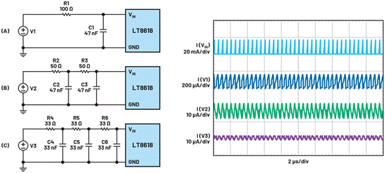
Figure 5. Current ripple on the power supply side of the current loop
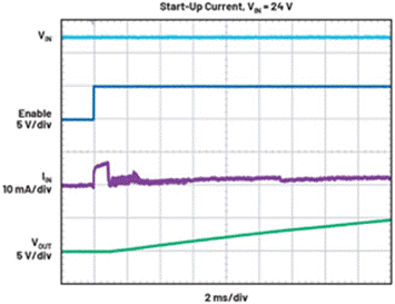
In a typical current loop application, the customer will specify a current limit during startup (e.g. 3.2 mA), but this limit can be exceeded in a specified short time. In buck converter, high impulse current is usually generated to charge input capacitor. The input filter has two functions: in addition to limiting the ripple current at the source side of the cable, it also helps to limit the impulse current when starting. Figure 6 shows the change of the input current with time during the startup of the two-stage input filter when the input voltage VIN is 24V and the output side load current is 4mA.
Figure 6. The starting current when using the input filter is used to limit the impact current (starting from the top: input voltage 20V/div, output voltage 5V/div, enable, input current at the cable side, 10mA/div)
conclusion
The current loop is widely used in industrial and automotive systems to collect sensor information and transmit it to the control system, sometimes through relatively long wires. On the contrary, the loop transmits controller output and modulation instructions to remote actuators and other devices. By improving the power supply in the current loop, especially replacing the traditional linear regulator with a high-efficiency step-down regulator, the efficiency and performance can be significantly improved, and the current capacity can also be enhanced and the input range can be expanded. The regulator with high efficiency and high input voltage adopts a small package, which has a low minimum conduction time and can achieve a compact overall solution. Its size and robustness can be comparable to that of LDO regulator solutions. This article describes how to use the LT8618 in a 4 mA to 20 mA current loop transmitter to meet strict industrial requirements.
About the author
Zhongming Ye is a chief application engineer of power supply products of ADI Company, whose working place is located in Santa Clara, California, USA. Since 2009, he has been working in Linglilte (now a part of ADI), responsible for providing application support for various products, including buck, boost, flyback and forward converters. His focus in the field of power management includes high-performance power converters and regulators with high efficiency, high power density and low EMI for automotive, medical and industrial applications. Before joining Linklatet, he worked in Intersil for three years, engaged in PWM controller related work of isolated power supply products. He holds a doctorate in electrical engineering from Queen‘s University in Kingston, Canada. Zhongming is a senior member of IEEE Power Electronics Institute.
Juan-G. Aranda is a design manager working in Munich. He joined ADI 16 years ago. Since then, he has designed a variety of general-purpose step-down regulators, industrial line drivers suitable for sensor applications, and active rectifier controllers for automotive systems. He recently developed the LT8618 and LT8604 series of new high efficiency step-down regulators for low output current applications. Juan holds a master‘s degree in telecommunications engineering from the Technical University of Valencia, Spain.
|
Disclaimer: This article is transferred from other platforms and does not represent the views and positions of this site. If there is any infringement or objection, please contact us to delete it. thank you!
中恒科技ChipHomeTek
|


 Service mailbox
 13823783658
 ChatNow