01 LDO margin and its influence on output noise and PSRR
The latest gigabit analog circuits based on deep submicron technology have lower and lower requirements for power supply voltage, which is less than 1V in some cases. These high-frequency circuits often require large power supply current, so there may be difficulties in heat dissipation. One of the design goals is to reduce the power consumption to the level absolutely required for circuit performance.
The switching mode DC-DC converter is an efficient power supply. The efficiency of some devices can exceed 95%, but the cost is power noise, which usually exists in a wide bandwidth range. Low dropout linear regulator (LDO) is usually used to eliminate the noise in the power rail, but it is also necessary to make a trade-off between power consumption and increased system heat load. In order to alleviate these problems, LDO can make the difference between input and output voltages smaller (margin voltage). This paper aims to discuss the influence of low margin voltage on power supply rejection and total output noise.
02 LDO power supply suppression and margin
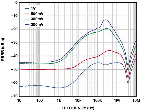
LDO power supply rejection ratio (PSRR) is related to margin voltage - margin voltage refers to the difference between input and output voltages. For fixed margin voltage, PSRR decreases with the increase of load current, especially under the conditions of large load current and small margin voltage. Figure 1 shows the PSRR of ADM7160 ultra-low noise 2.5V linear regulator under 200mA load current and 200mV, 300mV, 500mV and 1V margin voltage. As the margin voltage decreases, PSRR will also decrease, and the differential pressure may become very large. For example, at 100kHz, the margin voltage changes from 1V to 500 mV, resulting in a 5dB reduction in PSRR. However, a small change in margin voltage, from 500mV to 300mV, will result in a PSRR decrease of more than 18dB.
Figure 1. ADM7160 PSRR and Margin
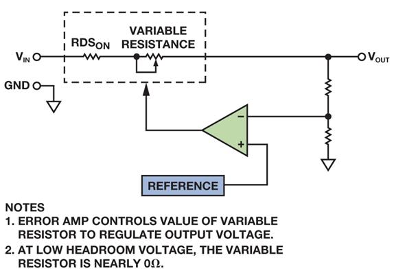
Figure 2 shows the block diagram of LDO. With the increase of load current, the gain of PMOS adjusting element will decrease, and it will break out of saturation state and enter the three pole working area. As a result, the total loop gain decreases, resulting in a decrease in PSRR. The smaller the margin voltage, the greater the gain reduction. As the margin voltage continues to decrease to a point, the gain of the control loop drops to 1 and the PSRR drops to 0dB.
Another factor that causes the loop gain to decrease is the resistance of the components in the path, including the on resistance of the FET, the on-chip interconnect resistance, and the solder wire resistance. The resistance can be calculated according to the pressure difference. For example, the ADM7160 packaged with WLCSP has a maximum differential pressure of 200mV at 200mA. Using Ohm‘s law, the resistance of the adjusting element is about 1 Ω, and the adjusting element can be approximately regarded as the sum of fixed resistance and variable resistance.
The voltage difference caused by the load current flowing through the resistor subtracts the drain source operating voltage of the FET. For example, under the condition of 1 Ω FET, the load current of 200 mA will reduce the drain source voltage by 200 mV. When estimating the PSRR of LDO with 500 mV or 1 V margin, the differential pressure on the adjusting element must be considered, because the operating voltage of the adjusting FET is actually only 300 mV or 800 mV.
Figure 2. Block Diagram of Low Differential Pressure Regulator
03 Effect of tolerance on LDO margin
Customers usually ask application engineers to help them select appropriate LDOs to generate low noise voltage X from input voltage Y under load current Z, but when setting these parameters, the input and output voltage tolerances are often ignored. As the margin voltage becomes smaller and smaller, the tolerance of input and output voltages may have a huge impact on the operating conditions. Worst case tolerances for input and output voltages always result in a drop in margin voltage. For example, the worst case output voltage may be 1.5% higher and the input voltage may be 3% lower. When a 3.3 V regulator is driven by a 3.8 V source, the worst condition margin voltage is 336.5 mV, much lower than the expected value of 500 mV. Under the worst load current of 200 mA, the drain source voltage of the FET is only 136.5 mV. In this case, the ADM7160 PSRR may be 55 dB below the nominal value (at 10 mA).
04 PSRR of LDO in differential pressure mode
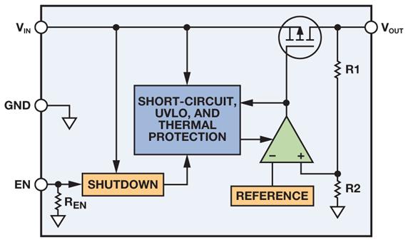
Customers often consult application engineers about LDO PSRR in differential pressure mode. At first, this seems to be a reasonable problem, but as long as you look at the simplified block diagram, you can see that this problem is meaningless. When LDO operates in differential voltage mode, the variable resistance part of the FET is adjusted to zero, and the output voltage is equal to the difference between the input voltage and the voltage drop caused by the load current of RDSON of the FET. LDO is not regulated, and there is no gain to suppress input noise; Just act as a resistor. The RDSON of FET and the output capacitor together form an RC filter to provide a small amount of residual PSRR, but a simple resistor or ferrite bead can complete the same task, and it is more cost-effective.
05 Maintain performance in low margin operation mode
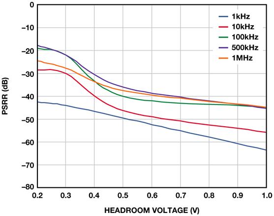
In the low margin operating mode, the influence of margin voltage on PSRR should be considered, otherwise, the output voltage noise level will be higher than expected. The relationship curve between PSRR and margin voltage shown in Figure 3 can usually be found in the data manual, and can be used to determine the noise suppression amount that can be achieved under given conditions.
Figure 3. Relationship between PSRR and margin voltage
However, sometimes it is easier to see the value of this information by showing how the PSRR of LDO can effectively filter the noise in the source voltage. The following graph shows the influence of LDO on the total output noise under different margin voltages.
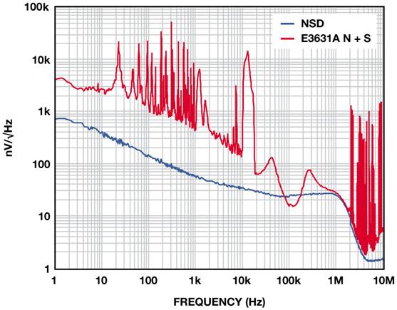
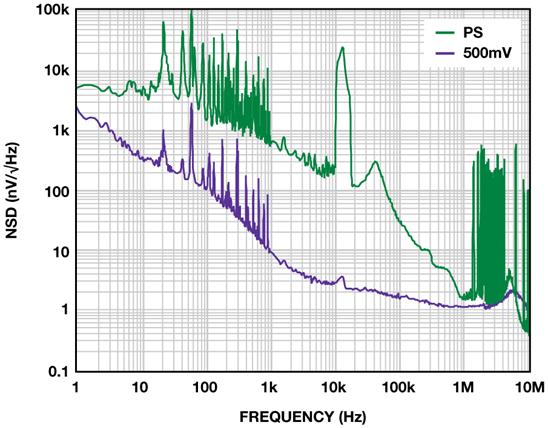
Figure 4 shows that under 500 mV margin and 100 mA load conditions, the rated noise of 2.5 V ADM7160 is less than 350 in the range of 20 Hz to 20 MHz compared with the output noise of E3631A desktop power supply μ V-rms。 Many spurs below 1 kHz are harmonics associated with 60 Hz line frequency rectification. The wide spurious above 10kHz comes from the DC-DC converter that generates the final output voltage. Stray above 1 MHz comes from RF sources irrelevant to power noise in the environment. In the range of 10Hz to 100kHz, the measured noise of the power supply used for these tests is 56 μ Vrms, including 104 stray μ V。 LDO suppresses all noises on the power supply, and the output noise is about 9 μ V-rms。
Figure 4. ADM7160 Noise Spectrum Density (500 mV margin)
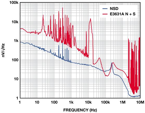
When the margin voltage drops to 200 mV, as the high-frequency PSRR approaches 0 dB, the noise spurious above 100 kHz starts to pass through the noise floor. The noise rises slightly to 10.8 μ V rms。 As the margin drops to 150 mV, the rectified harmonics begin to affect the output noise, which rises to 12 μ Vrms。 A moderate peak appears at about 250 kHz, so although the total noise increase is not large, the sensitive circuit may also be adversely affected. As the margin voltage decreases further, the performance is affected, and the spurious associated with rectification begins to appear in the noise spectrum. Figure 5 shows the output with a 100 mV margin. The noise has risen to 12.5 μ V rms。 The energy contained in harmonics is very little, so the stray noise only increases slightly, which is 12.7 μ V rms。
Figure 5. ADM7160 Noise Spectrum Density (margin of 100 mV)
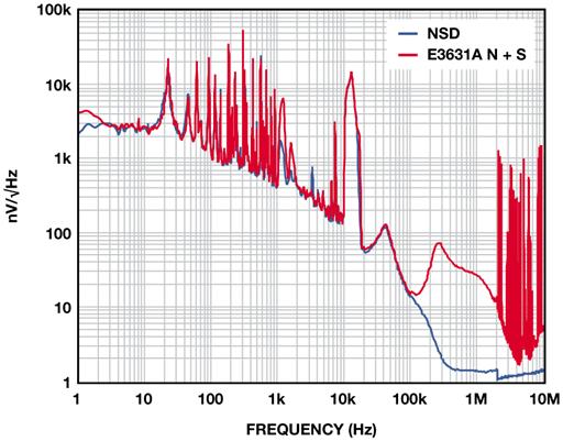
When the margin is 75 mV, the output noise is seriously affected, and the rectifier harmonics appear in the entire spectrum. Rms noise rises to 18 μ V rms, the sum of noise and spurious increases to 27 μ V rms。 Noise exceeding the range of~200 kHz is attenuated because the LDO loop has no gain and acts as a passive RC filter. When the margin is 65 mV, the ADM7160 operates in differential pressure mode. As shown in Figure 6, the output voltage noise of ADM7160 is actually the same as the input noise. Now rms noise is 53 μ Vrms, the sum of noise and stray is 109 μ V rms。 Noise beyond the~100 kHz range is attenuated because the LDO acts as a passive RC filter.
Figure 6. Noise Spectrum Density of ADM7160 in Differential Pressure Mode
06 High PSRR, ultra-low noise LDO
For example, new LDOs such as ADM7150 ultra-low noise and high PSRR regulators are actually connected with two LDOs. Therefore, the PSRR obtained is about the sum of each stage. These LDOs require a slightly higher margin voltage, but can achieve PSRR of more than 60 dB at 1 MHz, and PSRR can be far more than 100 dB at lower frequencies.
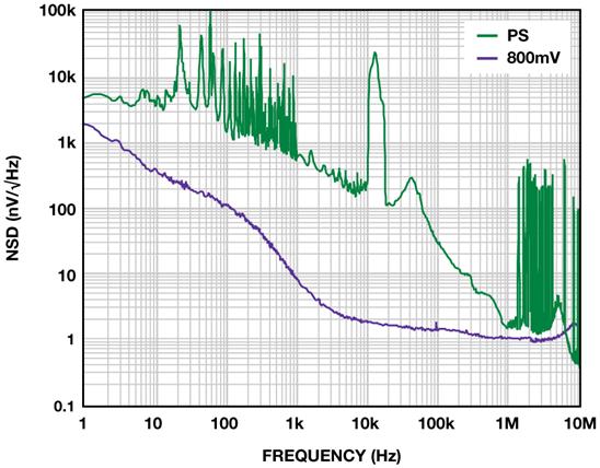
Figure 7 shows the noise spectrum density of a 5 V ADM7150 with a load current of 500 mA and a margin of 800 mV. Output noise is 2.2 in the range of 10 Hz to 100 kHz μ V rms。 As the margin decreases to 600 mV, the rectifier harmonics begin to appear, but when the output noise rises to 2.3 μ V rms, its influence on noise is very small.
Figure 7. ADM7150 Noise Spectrum Density (800 mV margin)
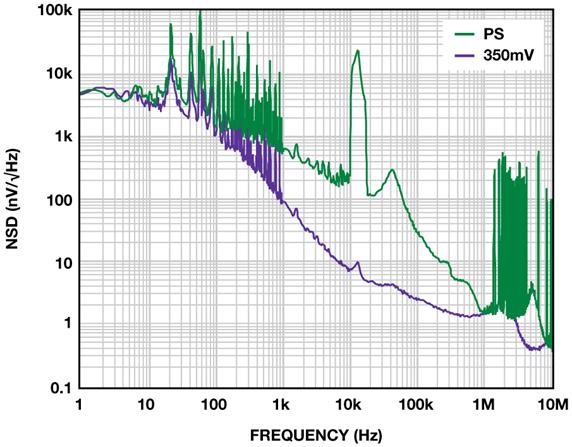
When the margin is 500 mV, the rectified harmonics and peaks can be seen at 12 kHz, as shown in Figure 8. Output voltage noise rises to 3.9 μ V rms。
Figure 8. ADM7150 Noise Spectrum Density (500 mV margin)
When the margin is 350 mV, LDO adopts differential pressure operation mode. At this time, the LDO can no longer adjust the output voltage, acting as a resistor, and the output noise rises to nearly 76 μ V rms, as shown in Figure 9. Only the poles formed by the RDSON of the FET and the capacitor at the output end attenuate the input noise.
Figure 9. Noise Spectrum Density of ADM7150 in Differential Pressure Mode
07 Conclusion
Modern LDO is increasingly used to eliminate the noise in power rails, which are usually realized by switching regulators that can generate noise in a wide spectrum. The switching regulator forms these voltage rails with ultra-high efficiency, but the energy consuming LDO itself will not only reduce noise, but also lead to efficiency degradation. Therefore, the operating margin voltage of LDO should be reduced as much as possible.
As mentioned earlier, PSRR of LDO is a function of load current and margin voltage, which will decrease with the increase of load current or the decrease of margin voltage, because when the operating point of the regulator is moved from the saturated operating area to the three pole operating area, the loop gain will decrease.
By considering the input source noise characteristics, PSRR and worst-case tolerance, designers can optimize power consumption and output noise to create an efficient low-noise power supply for sensitive analog circuits.
Under the condition of ultra-low margin voltage, the worst condition tolerance of input and output voltage may affect PSRR. Fully considering the worst condition tolerance during design can ensure reliable design. Otherwise, the total noise of the power supply solution designed with low PSRR will also be higher than expected.
|
Disclaimer: This article is transferred from other platforms and does not represent the views and positions of this site. If there is any infringement or objection, please contact us to delete it. thank you!
中恒科技ChipHomeTek
|

 Service mailbox
 13823783658
 ChatNow