By Frederik Dostal, ADI Field Application Engineer
A boost converter is used to generate a high output voltage from a low input voltage. This voltage conversion can be easily achieved using switching regulators and boost topologies. However, the voltage gain itself has limitations. The voltage gain is the ratio of the output voltage to the input voltage. If 24V output voltage is generated from 12V input voltage, the voltage gain is 2.
Taking an industrial application as an example, it is necessary to generate 300V output voltage from 24V power supply voltage, and the output current is 160mA.
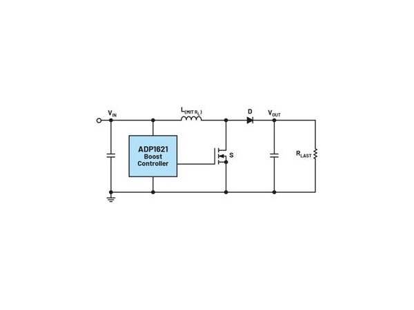
Figure 1. Boost converter circuit
The duty cycle can also be used to express the voltage gain:
The duty cycle and voltage gain are the main parameters of the boost converter. The duty cycle represents the length of time that switch S is open in each cycle. The voltage gain represents the proportion (factor) by which the output voltage exceeds the input voltage.
In order to generate a high voltage, the duty cycle value will increase to close to 1, but will not reach 1.
Selecting a boost converter with a high maximum duty cycle seems to generate a high output voltage from a low supply voltage. However, this is not the only determinant. In addition to the duty cycle limitation, the maximum possible voltage gain must also be considered.
The voltage gain is the ratio of the maximum possible output voltage of the boost converter to the available input voltage. The limitation of the boost converter itself can be understood in this way: when using the boost converter, all electric energy must be temporarily stored when it is transferred from the input to the output. During the opening, that is, during the opening of switch S in Figure 1, the electric energy will be temporarily stored in the inductor L. At this time, diode D in Figure 1 blocks the current flow.
During shutdown, the electrical energy temporarily stored in inductor L will discharge. Inductance charging and discharging must follow the inductance rules. In each case, the current is determined by the inductance value and the voltage difference between the two ends of the inductance. The voltage at both ends of the inductor can be simply described as VIN during charging and VOUT - VIN during shutdown.
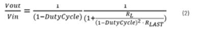
When the voltage gain is high, the closing time may not be long enough, resulting in that the electrical energy temporarily stored in the inductor cannot be discharged completely. Therefore, the simplified formula describing duty cycle in Formula 1 cannot express this limitation. The maximum voltage gain formula is valid only when the DC resistance (DCR) of the inductor and the load resistance are considered simultaneously. See Formula 2:
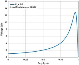
Therefore, the ratio of RL to RLOAD will affect the ratio between the possible input and output voltages, thereby affecting the voltage gain of the boost converter. The voltage gain can be as shown in the figure. In the example shown in Figure 2, the input voltage is 24V, the output voltage is 300V, the current is 160mA, the load resistance is 1.8k Ω, and the DCR of the inductance RL is 3 Ω.
Figure 2. Possible voltage gain when load resistance reaches 600 times of inductance DCR (RL)
In this example, Fig. 2 shows that the voltage gain may reach about 12.5 (calculated according to Formula 2). However, if the load resistance decreases (that is, the output current increases), or the DCR (RL) of the inductor increases (that is, the size of the inductor decreases), the required voltage gain will not be achieved.
Figure 3 shows the voltage gain curve when the ratio of load resistance to inductance resistance is 300. At this time, select RL as 6 Ω and load resistance as 1.8k Ω.
Figure 3. Possible voltage gain when load resistance reaches 300 times of inductance DCR
Figure 3 shows that in this case, the maximum voltage gain is only 9. Therefore, it is impossible to convert 24V input voltage to 300V output voltage. The selected DCR or inductance RL is too high.
In conclusion, when designing a circuit with boost topology, it is important to determine the maximum possible voltage gain. It should be noted that it depends on the DCR of load resistance (i.e. output current) and inductance. If it appears that the required voltage gain cannot be achieved, a larger inductor with a lower DCR can be selected.
About ADI
Analog Devices, Inc. (NASDAQ: ADI), a world leading semiconductor company, is committed to building a bridge between the real world and the digital world to achieve breakthrough innovation in the intelligent edge field. ADI provides solutions that combine analog, digital and software technologies to promote the sustainable development of digital factories, automobiles, digital medicine and other fields, address the challenges of climate change, and establish a reliable interconnection between people and the world. ADI‘s revenue in fiscal year 2022 will exceed 12 billion US dollars, with more than 24000 employees worldwide. Together with 125000 customers worldwide, ADI helps innovators continuously surpass all possibilities. For more information, please visit www.analog.com/cn.
About the author
Frederik Dostal studied microelectronics at Erlangen University in Germany. He began to work in 2001 and set foot in the power management business. He once held various application engineer positions, and worked in Phoenix, Arizona for four years, responsible for switching mode power supply. He joined ADI in 2009 and worked as a field application engineer for power management at ADI in Munich.
|
Disclaimer: This article is transferred from other platforms and does not represent the views and positions of this site. If there is any infringement or objection, please contact us to delete it. thank you!
中恒科技ChipHomeTek
|


 Service mailbox
 13823783658
 ChatNow