1 Introduction
Switching power supply is one of the focuses of the power supply market in recent years. Its biggest advantage is to reduce the volume and weight of the transformer greatly, thus reducing the volume and weight of the entire system. Generally speaking, the weight of switching power supply is 1/4 of that of linear power supply, and the corresponding volume is about 1/3 of that of linear power supply. Therefore, switching power supply poses a threat to low-grade linear power supply, especially linear power supply below 20W, and has the potential to replace it. However, in addition to PWM and power MOSFET, the traditional switching power supply also includes about 50 discrete components, which not only increases the cost and volume, but also affects the reliability. This is mainly due to the production process. There has been no breakthrough in the integration of switching power supply.
In recent years, with the maturity of production technology, low-voltage control unit and high-voltage high-power tube can be integrated into the same chip. TI, ON SemIConductor, Power, Integrations and other companies have similar products, while there is almost no domestic market. Due to the advantages of switching power supply in volume, weight, efficiency and reliability, its research and development speed is amazing.
Its main application fields include: ① post and telecommunications: as a program-controlled exchange, mobile communication base station power supply; ② Computer: used as switching power supply for various PCs, servers and industrial control machines; ③ Household electronic products: At present, the household electronic products that use switching power supply include TV sets, DVD players, etc.; ④ Other industries: such as electric power, aerospace, military and other fields.
According to the process development and market demand, the core power MOSFET and low-voltage PWM controller are integrated into one chip. At the same time, it also has the functions of overheat protection, overvoltage protection, undervoltage locking, automatic restart, overcurrent protection, etc. This new type of switching power supply integrated circuit has brought many advantages to the power supply system. The AC input of the chip can be directly connected from the power grid, with low power consumption, low cost and small size. At the same time, it also improves the stability of the system, reduces the cost, and makes the design of electronic engineers more simple. The chip can be used to drive a single-ended grounding power supply system, such as outputting a DC voltage after connecting a secondary coil transformer with oscillating flyback.
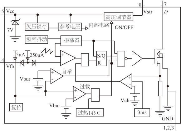
2 Working principle
This switching power supply is an IF integrated module with a design frequency of 100kHz and a maximum duty cycle of 70%. It includes a constant frequency pulse width modulator and a high integration power supply switching circuit. Its structure is shown in Figure 1. The high-voltage side of the combined switch can continuously control the AC voltage from 85 to 265V, which can be applied to most conventional power supply systems.
Through a photoelectric coupling tube, the load change is fed back to the chip. The feedback signal generates a voltage drop on the 2.7k resistance. Through a 7kHz low-pass filter, the high-frequency switching noise is filtered out, and is input to the PWM module in the form of DC voltage for regulation. The pulse wave whose duty cycle changes with the feedback signal is generated. The power MOSFET is driven by the drive circuit, thus realizing PWM regulation. In addition, the source pole of the power MOSFET is connected with a resistor to realize current limiting protection for each cycle.
Under normal conditions, the output signal of 1/8 frequency divider makes the power MOSFET turn on. If a fault occurs, its output signal makes the power MOSFET turn off, and it starts counting itself. In the first cycle, the power MOSFET turns on. If it is not eliminated, it will continue to circulate according to this law; If the fault is eliminated, it will enter the normal working state. The IC is externally connected with a transformer. After realizing the AC-DC function, different specifications of transformers can obtain different DC voltages.
3 Introduction to internal function modules
3.1 Oscillator circuit
As shown in Figure 2, the oscillator uses two comparators to turn on, charge and discharge the capacitor, and obtain a sawtooth wave oscillating at the voltage of 2.7~4.1 V. Its design frequency is 100kHz and its duty cycle is 70%. When charging and discharging capacitors, constant current charging and discharging can be realized by using the principle of constant working current in the saturation region of MOS tubes. The equivalent simplified circuit model is shown in Figure 3. When charging, switch S is closed to end 3, DQ="DU" can be obtained × C (1) and DU=4.1-2.7=1.4v (3)
In the formula, C=40pF, IP="18". 6mA, T P="3ms" can be calculated. When discharging, when the switch S is turned to the 8 terminal, IN=8mA, TN=7ms can be calculated.
T="Tp"+T N="10ms" (5)
The design of the duty cycle also needs to be considered. When the duty cycle is increased, the power efficiency of the whole IC and external circuits will be improved. However, it cannot be infinitely improved to close to 100%, which is mainly due to the time limit of the establishment and recovery of transformer magnetic flux. At the same time, the power MOSFET is easy to burn out after a long time of conduction.
3.2 Bias circuit
The circuit uses a three-tube bandgap reference power supply, as shown in Figure 4. The emitter voltage of T2 is shown in formula (6). It can be seen from the formula that the positive temperature coefficient of the equivalent thermal voltage Vt and the negative temperature coefficient of Vbe can be mutually compensated to make the temperature coefficient of the output reference voltage close to zero (because the Vbe of T6 and T2 are the same, the output voltage Vref and T2 emitter voltage are the same).
3.3 PWM modulation circuit
The signal coupled by the optocoupler to reflect the load change first passes through a 7kHz low-pass filter, and then sent to the PWM comparator and the sawtooth wave generated by the oscillator for comparison, so as to realize pulse width modulation. The frequency response of the low-pass filter is
It can be used as a design parameter.
3.4 Overvoltage protection, undervoltage locking circuit
The working voltage environment of the designed internal circuit is 7.5~8.6V. The circuit is shown in Figure 5 and consists of comparators C1, C2 and resistors R1, R2, R3 and R4. Due to the hysteresis comparator, when Vcc is at 7.5~8.6V, the IC operates normally. When Vcc>8.6V, C1 outputs a high level, which directly turns on the discharge NMOS tube for discharge. The NMOS tube is designed to be relatively large, which can discharge quickly and make the IC return to the safe state in time. If the Vcc fault still exists, it will be counted with an octave counter. This octave counter turns off the power MOSFET, and the capacitor will be charged and discharged repeatedly in 8 consecutive cycles. After 8 cycles, if the fault is eliminated, the whole IC will enter the normal working state, and the power MOSFET will be turned on. This design can greatly reduce the dissipation power of power MOSFETs. When the internal working voltage Vcc<7.5V, C1 outputs a low level, turns off the drive, and drives the high-voltage starting circuit, which is connected externally by 10 μ F capacitor for charging. At the same time, the low level is also sent to the counter for counting, thus realizing the self-starting function. Generally speaking, Vcc<7.5V is caused by the loss of output voltage of the additional coil of the power transformer caused by load short circuit or overload, and there is not enough voltage to supply power to the chip.
3.5 Thermal shutdown circuit
The thermal shutdown circuit is shown in Figure 6. Under normal conditions, T=25 ℃, Vz=6.3V, V BE1=0.75V, VBEH=0.65V, at this time, VH=R3 (Vz - VBE1)/(R2+R3)=0.43V<VBEH
Therefore, Q1 is not conductive, so Vout is high.
In fault state, the temperature coefficient of the voltage regulator is positive, while the VBE of the transistor is negative. The designed temperature protection capacity (when T=150 ℃) is
It is also calculated that VH (150 ℃)=0.46V, so Q 2 is on and Vout is low. This signal directly turns off the power MOSFET. At the same time, this pulse signal is also input to the 1/8 frequency divider for counting.
3.6 High-voltage starting circuit
The high-voltage starting circuit is shown in Figure 7. When the IC is powered on, the whole IC is in the state of establishing the working environment. If the gate of VDMOS is high, the tube is on and there is charging current at the Out end. When Vcc reaches 8.6V, the signal Vstart sent by the overvoltage protection circuit is a low level, making P2 conductive, so that the VDMOS is cut off. In addition, R1 is used to make P1 and Q1 turn on when the charging current is too large, so as to cut off the VDMOS and play a protective role. The design value of this charging current capacity is 3mA. If it exceeds this value, the VDMOS will stop. According to the calculation, the time required for the whole IC to establish the working environment is 40ms, which is consistent with the actual simulation results.
3.7 Drive circuit
The drive circuit is designed to remove the burr of the drive signal and protect the gate of the power MOSFET (Fig. 8). Under normal conditions, N1, N2 and N3 are in cut-off state. When the internal power supply voltage Vcc of the circuit suddenly changes from low level to high level, the voltage at both ends of the capacitor C cannot be sudden changed, so that N1 is on and the output is 0. In addition, when the IC is suddenly powered on, the gate voltage is high due to the existence of the gate drain capacitance of the power MOSFET. However, due to the existence of resistors R and N3 added in the design, the gate is bypassed to play a protective role. Finally, if the IC is suddenly powered off, there is no large current supply for the power tube drain. If the drive is at high level at this time, the current can be unloaded from R, and finally the low level will become low. In short, N1, N2 and N3 protect the gate of power MOSFET.
3.8 Leading edge blanking circuit
The leading edge blanking circuit is shown in Figure 9. Under normal conditions, if the voltage at point A is low and the 2 tubes are on, the C2 output is high; In case of fault, that is, when the current of the power MOSFET is too large, the potential of point A will rise, making the 2 tubes turn off, so that the C2 output will be low level and fault pulse will occur. It is worth mentioning that the grid input signal of the 2-transistor and its source input signal are not synchronized. The advantage of this design is that it can avoid excessive current in a short time. If the current is always large, it can play a leading role in blanking. The delay size of these two signals is composed of several stages of inverters and capacitors, of which the capacitor is the largest contributor, and its design delay time is 200ns.
4 Simulation results
During the simulation, the normal operation, overvoltage, undervoltage, overcurrent, overload and other conditions are analyzed. Figure 10 simulates the change of power MOSFET output when the load changes. The bottom waveform is the voltage after the load condition passes through the optical coupling and low-pass filter, the middle waveform is the IC internal voltage Vcc signal, and the top waveform is the drive voltage signal on the power MOSFET gate. It can be seen that due to charging, Vcc will not increase when it reaches 8.6V (overvoltage protection
Figure 11 simulates the situation when the IC internal voltage is abnormal. The bottom wave is the gate drive voltage of the power MOSFET, the middle wave is the working signal (Vstart) of the automatic restart circuit, and the top wave is the internal voltage Vcc signal of the IC. It can be seen that when Vcc rises to 8.5V, the automatic restart circuit is closed, and the counter starts counting. At this time, the power MOSFET is still in operation. When Vcc decreases to 7.5V, the automatic restart circuit starts to work, and the external connection is 10 μ F capacitor for charging. This is repeated for 8 times. At the ninth cycle, the power MOSFET works again, meeting the initial design requirements.
5 Conclusion
This paper designs an IC of power switching power supply for portable equipment. Through the analysis of its functions and characteristics, the circuits of each sub-module are designed and simulated. The results show that the load regulation is sensitive and accurate, and all kinds of protection circuits act timely and reliably.
|
Disclaimer: This article is transferred from other platforms and does not represent the views and positions of this site. If there is any infringement or objection, please contact us to delete it. thank you!
中恒科技ChipHomeTek
|

 Service mailbox
 13823783658
 ChatNow