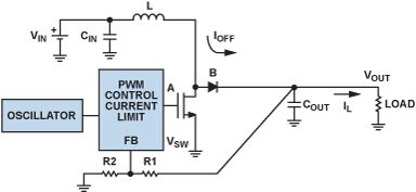
The voltage regulator using Schottky diode instead of switch B is defined as asynchronous (or asynchronous), while the voltage regulator using FET as switch B is defined as synchronous. In Figure 3, switches A and B are realized by internal NFET and external Schottky diodes respectively to create asynchronous boost voltage regulator. For low-power applications requiring load isolation and low turn-off current, external FETs can be added, as shown in Figure 4. Drive the EN pin of the device below 0.3 V to turn off the voltage regulator and completely disconnect the input and output.
Figure 4. Typical application circuit of ADP1612/ADP1613.
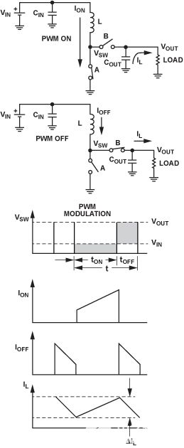
Modern low-power synchronous step-down regulators use pulse width modulation (PWM) as the main operating mode. PWM keeps the frequency constant and changes the pulse width (on t) to adjust the output voltage. The average power provided is proportional to the duty ratio D, making it an effective way to supply power to the load.
For example, for the required output voltage of 15 V and the available input voltage of 5 V,
D=(15 – 5)/15=0.67 or 67%.
Energy is conserved, so the input power must be equal to the power delivered to the load minus any loss. Assume that the conversion is very
For example, if the load current is 300 mA at 15 V, I=900 mA at 5 V - three times the output current. Therefore, the available load current decreases with the increase of boost voltage.
The boost converter uses voltage or current feedback to adjust the selected output voltage; The control loop enables the output to remain regulated in response to load changes. The operating frequency of low power boost regulators is usually between 600 kHz and 2 MHz. A higher switching frequency allows the use of smaller inductors, but the efficiency will decrease by about 2% each time the switching frequency is doubled. In the ADP1612 and ADP1613 boost converters (see appendix), the switching frequency can be selected through pins. The operating frequency is 650 kHz to achieve the maximum efficiency, and the operating frequency is 1.3 MHz to achieve the minimum external components. Connect FREQ to GND to achieve 650kHz operation, or connect to VIN to achieve 1.3-MHz operation.
The inductor is the key component of the boost voltage regulator, which stores energy during the power switch on, and transmits this energy to the output terminal through the output rectifier during the power switch off. In order to balance the balance between low inductance current ripple and high efficiency, the ADP1612/ADP1613 data manual recommends that the inductance value be 4.7 μ H to 22 μ H range. Generally, for a given physical size, a lower value of inductance has a higher saturation current and a lower series resistance, but a lower value of inductance will lead to a higher peak current, resulting in lower efficiency, increased ripple and increased noise. Generally, it is best to operate the boost in the discontinuous conduction mode to reduce the inductance size and improve the stability. The peak inductive current (the maximum input current plus half of the ripple current of the inductor) must be lower than the rated saturation current of the inductor; The maximum DC input current of the voltage regulator must be less than the rms rated current of the inductor.
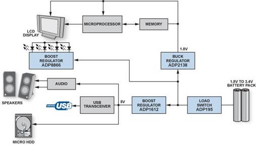
Specifications and definitions of main booster and voltage stabilizer
Input voltage range: The input voltage range of the boost converter determines the lowest available input power supply voltage. The specification may display a wide input voltage range, but the input voltage must be lower than V to achieve efficient operation.
Grounding or quiescent current: DC bias current (I q) not transmitted to the load. The lower I q, the better I q efficiency. However, I q can be specified under a variety of conditions, including turn-off, zero-load, PFM operation or PWM operation. Therefore, it is better to check the operating efficiency under specific operating voltage and load current to determine the best boost voltage regulator suitable for application.
Turn off current: the input current consumed when the enable pin is set to turn off. Low self q is very important for the long standby time when the battery powered device is in sleep mode.
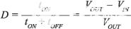
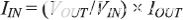
Switch duty cycle: the working duty cycle must be lower than the maximum duty cycle, otherwise the output voltage will not be adjusted. For example, D=(V out – V in)/V out. Following V in=5 V and V out=15 V, D=67%. The maximum duty cycle of ADP1612 and ADP1613 is 90%.
Output voltage range: the output voltage range that the device will support. The output voltage of the boost converter can be fixed or adjustable. Use a resistor to set the required output voltage.
Current limit: The boost converter usually specifies the peak current limit instead of the load current. Please note that the greater the difference between the two, V outside and V, the lower the available load current. The maximum available output current is set for the peak current limit, input voltage, output voltage, switching frequency and inductance value.
Line adjustment rate: The line adjustment rate is the change of output voltage caused by the change of input voltage.
Load regulation rate: The load regulation rate is that the output voltage changes with the output current.
Soft start: The boost voltage regulator must have a soft start function, which ramps up the output voltage in a controlled manner during startup to prevent the output voltage overshoot during startup. The soft start of some boost converters can be adjusted by external capacitors. When the soft start capacitor is charged, it will limit the allowable peak current of the device. Through adjustable soft start, the start time can be changed to meet the system requirements.
Thermal shutdown (TSD): If the junction temperature rises above the specified limit, the thermal shutdown circuit will shut down the voltage stabilizer. The continuous high junction temperature may be the result of high current operation, poor circuit board cooling or high ambient temperature. The protection circuit includes hysteresis, so the device will not return to normal working state until the in-chip temperature drops below the preset limit after thermal shutdown.
Undervoltage lockout (UVLO): If the input voltage is lower than the UVLO threshold, the IC automatically turns off the power switch and enters the low power consumption mode. This can prevent potential unstable operation under low input voltage and prevent power devices from conducting when the circuit cannot be controlled.
conclusion
The low-power boost regulator eliminates the worries of switching DC-DC converter design by providing a proven design. Design calculations can be found in the application section of the data manual and ADIsimPower. 4 Design tools simplify the tasks of end users.
|
Disclaimer: This article is transferred from other platforms and does not represent the views and positions of this site. If there is any infringement or objection, please contact us to delete it. thank you!
中恒科技ChipHomeTek
|


 Service mailbox
 13823783658
 ChatNow