There are many possible design methods for small antennas based on PCB. The most common is the use of open wire (also known as open) structures (such as bipolar and monopole antennas), loop design (such as loop antennas), and solid block design.
Open-ended antenna is actually a miniature version of the large antenna that has existed since the beginning of radio technology. In fact, because Heinrich Hertz used a bipolar antenna in his 1888 experiment, it is sometimes called Hertz antenna. It is balanced with the ground plane. Before the emergence of cable and satellite television, it has been faithfully performing the duties of VHF TV rabbit ear antenna.
Contrary to bipolar antenna, monopole antenna is single-ended to the ground, so a ground plane is required. In many wireless applications, monopole antennas are used as whip antennas. It is also known as Marconi antenna, which was used in Marconi‘s early experiments.
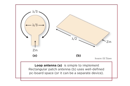
Figure 1: The ring antenna (a) is easy to implement. Rectangular block antenna (b) uses well planned PCB space (it is also a discrete device)
Ring antennas used in mass markets such as UHF TV also have a long history. Its circumference is approximately equal to the wavelength of the signal that can be received (see Figure 1a). In terms of electrical characteristics, the rectangular block antenna is a relatively wide microstrip transmission line, and its length is half of the working wavelength. In Figure 1b, the wavelength is not calculated by propagation in vacuum, but by insulating PCB material. The resonance frequency band of the rectangular block is quite narrow, so its working bandwidth is also quite narrow - about 5% of the nominal center frequency. Whether this characteristic is good or bad depends on the specific application.
All three types of antennas can be realized with PCBs, and a multi-layer PCB can provide multiple design options, including the ground plane required for certain structures. This antenna design is used in applications such as remote control unlocking (RKE) and garage opener that do not require strict performance requirements.
Since the design cost of PCB antenna is negligible, when and why is it not a design priority? Several of these dominant factors are related to front-end design and actual implementation.
First of all, antenna design is not simple. Even with modeling procedures such as Digital Electromagnetic Code, circuit or system engineers are unfamiliar with the electromagnetic world. They are facing a world of electromagnetic fields, rather than specific voltage and current points or the flow of electrons in a fixed circuit.
Secondly, like many engineering designs, the competing and conflicting attributes such as center frequency, bandwidth, field mode, efficiency, organization and gain make it difficult to balance them.
Third, it is not easy to evaluate the antenna performance. It requires special test instruments, non-reflective chambers or open areas. It also requires time, money and expertise. In addition, when evaluating the impact of the user‘s hand on the antenna, or conversely, when evaluating the impact of antenna radiation on the user‘s hand, correct test settings should be made, including the physical copy of the human hand and head.
And these are all theoretical. In fact, there are other factors at work. Of course, the antenna occupies PCB space, and its performance properties are significantly affected by nearby devices and users‘ hands, heads and bodies. The relative dielectric constant of human tissue is 40, while the dielectric constant of PCB components is about 25 to 85, so human tissue will stimulate resonance elements and affect the magnetic field.
In addition, when multiple antennas are required for multi-band operation or shape diversity design, the interaction between several PCB-based antennas and between antennas and adjacent areas will make performance prediction very difficult, and it is sensitive to subtle layout changes.
However, there are also rules that restrict the SAR of the antenna field. SAR is the ratio of RF absorption capacity of mass (human tissue in this case); Two methods are usually used to measure it: one is to measure the temperature rise caused by absorption; The second is to measure the electric field of fluid simulating human tissue. More information is available on the FCC website. It is necessary to understand and analyze the near-field and far-field performances of antennas, which may be closely related.
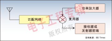
Finally, the antenna is not isolated from the receiving front-end or transmitting power amplifier stage of the wireless device. The circuit designer must determine the impedance of the antenna and the correlation level, and then design a matching network to maximize power transmission within the entire target bandwidth (see Figure 2).
Figure 2: Antenna subsystem includes front-end receiving amplifier or transmitting amplifier, matching network and antenna itself.
This is usually a difficult design work, involving professional calculation and measurement as well as special tools. For example, Smith circle chart is required.
Dielectric becomes part of antenna design
Fortunately, the development of material science and antenna theory provides design engineers with other options besides external and PCB-based antennas. These antennas maximize the volume efficiency of the antenna, and at the same time overcome or actually eliminate the influence of layout and the uncertainty of matching. In contrast, blocky and whiplash wireless are two-dimensional, and their efficiency mainly depends on the space rather than the volume. Although discrete antennas actually increase the cost, they often reduce the size while improving or ensuring the performance of the product.
It may sound unreasonable. As an insulator, dielectric will play an important role in antenna design and implementation. But it is true that for more than 50 years, dielectric has been a part of antenna design, which helps to shape and manage antenna mode electric field. Field energy is accumulated and stored in the dielectric at a relatively high density, so external objects or fields have relatively small influence and do not affect the inherent resonance of the antenna.
Of course, high relative permittivity is only one of the key factors for the success of dielectric-based antennas. Materials also need low dielectric loss (high Q materials) and low temperature coefficient to minimize physical scale variation, which can lead to detuning.
For example, the Geohelix antenna of Sarantel in the UK uses unique ceramic materials and shapes. Compared with the block and whip antennas, it has the ability to reduce the near-field radiation by at least 90%. The near field affected by the user‘s hands and body is almost completely enclosed in the Sarantel antenna. The antenna is used as a band-pass filter to suppress out-of-band signals and also remove the ground plane on the PCB or chassis.
The ground plane is no longer needed because the design has balanced current. Since the total current flowing into the antenna is zero, its resonance is independent of PCB or package. In contrast, a microstrip based block or external whip antenna needs a ground plane to obtain resonance, and the current flowing into (or out of) the antenna needs to generate a complementary current on the ground plane to generate resonance.
Similarly, another British company, Antenova, has a high dielectric antenna technology, which provides a volumetric non-sympathic antenna suitable for omnidirectional, directional and even multi-band applications and has the advantages of frequency response characteristics above 10GHz. These high efficiency devices have relative immunity to the effect of near mismatch. These devices can be integrated to create a smart antenna with excellent maneuverability. Smart antennas are increasingly used in base stations to expand system capabilities and improve the performance of each call.
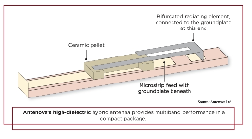
For example, Antenova has developed a dual-band hybrid IEEE 802.11a/b/g antenna for wireless LAN, covering 2.4 to 2.5 GHz and 4.9 to 5.9 GHz dual-band, which has 4 × four × 20 mm volume (see Figure 3).
Figure 3: Antenova‘s high dielectric hybrid antenna provides multi-band performance in a compact package
The antenna has three elements: a microstrip feeder, which also matches the 1.2mm diameter, ultra-small coaxial cable feeder connected to the antenna; A transmitting device, consisting of 1/4 wavelength block and two resonators (one for each frequency band); And a ceramic particle, which is responsible for exciting the transmitting element and forming coupling between the transmitting element and the feeder.
Different methods
Not all these new antennas are based on ceramics. Fractus in Barcelona uses the geometric model based on irregular fragment geometry in its antenna in-package design. The multi-band antenna can be printed on the substrate or embedded in the chip. They provide a GSM antenna with transmission efficiency higher than 70%, peak gain higher than 1dBi and VSWR lower than 1.5:1. The antenna has an unbalanced impedance of 50 ohms and a volume of only 10 × ten × 0.9mm。
As a comparison between block and discrete antennas from the same supplier Centurion Wireless Technology (now part of Laird Technologies), Centurion provides a microstrip block antenna that can be attached to the product shell. It works in the 2.4 to 2.5GHz frequency band, 43 × forty-three × 1.65mm size. In the operating frequency band, the antenna has a gain of 5.1dBi and a VSWR of less than 2.5:1. The gain of BlackChip surface-mount antenna in the same frequency band of Centurion is greater than 2dBi, and the VSWR is less than 2:1, 8 × six × 2.4mm size.
Most books on antenna design are full of complex theories and formulas that are difficult to use in practical design. However, this phenomenon is mainly due to the original characteristics of the antenna problem rather than the author‘s intention to appear obscure and profound. Small Antenna Design, written by Douglas B. Miron, published by Newnes/Elsevier, is a reference book covering theory, simulation and design.
|
Disclaimer: This article is transferred from other platforms and does not represent the views and positions of this site. If there is any infringement or objection, please contact us to delete it. thank you!
中恒科技ChipHomeTek
|

 Service mailbox
 13823783658
 ChatNow