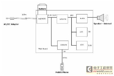
3.1.1) Sort out each power circuit, separate analog ground and digital ground, and do not cross each unit circuit. The digital ground and analog ground of BQ24133 are wired separately and connected to a single point through a 0 ohm resistor under the chip. In addition, the power ground of BQ24133 should be appropriately separated from the ground of the entire product and connected at a single point.
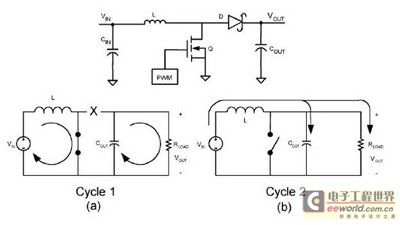
3.1.2) Reduce the area of the harmonic circuit. For LM3478, as shown in the figure, when the MOS transistor is turned on, Cin, L, and MOS form a circuit to charge the inductor. Please refer to Cycle1 in Figure 2 (a). When the MOS transistor is turned off, Cin, L, D, Cout form another circuit to discharge the inductance, as shown in Cycle2 in Figure 2 (b). For diode D, it operates alternately in the forward conduction and reverse cutoff states, so there is a high reverse recovery peak voltage. Snubber circuits need to be added at both ends of the diode to suppress this peak voltage to avoid generating excessive common mode noise. The working frequency of these two circuits is the switching frequency of MOS, and the harmonic component is large. When arranging the board, it is necessary to minimize the area of the harmonic circuit as much as possible. To place the components of these two power circuits close together, use a wide copper wire to reduce the circuit impedance of switching frequency harmonics.
Figure 2: LM3478 working principle diagram
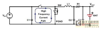
BQ24133 is essentially a Buck circuit. There are also similar issues. Please refer to Figure 3, the working principle diagram of BQ24133. The input capacitor C1, the rectifier tube on, the freewheeling tube off, the rectifier tube inductance and load form a high-frequency circuit, with a high dI/dT. In addition, when the rectifier is turned off and opened, the inductor current continues to flow through the coil (which operates in the continuous inductor current mode during heavy loads). When the inductor current does not decrease to zero, the rectifier will open again. This is because the coil is forced to apply a reverse voltage and cut off, resulting in a high reverse recovery voltage peak (although synchronous rectification, due to the existence of a dead time, diode rectification is still used during the dead time), This will result in relatively large common mode noise, so it is necessary to add a Snubber circuit in SW to PGND to suppress the reverse spike of the freewheeling tube. Therefore, the input filtering capacitor C1, inductor L1, and output filtering capacitor C2 should be arranged as close as possible to the chip to reduce the high-frequency circuit area. The power circuit wiring should be routed with a large copper sheet width to reduce harmonic impedance, preferably arranged on the same layer as the PCB, with the Snubber placed close to the lower tube.
Figure 3: BQ24133 High frequency current circuit diagram
Overall, the input and output of LM3478 and BQ24133 run through a large copper sheet, placing the input and output capacitors close to the power switch transistor to minimize the area enclosed by the circuit. The capacitor with smaller ESR is selected. Because of the cost, the capacitor used in this kind of products is relatively poor. This project used to use electrolytic capacitor, and it is recommended to add more ceramic chip capacitors for combination use, so as to achieve good results at low cost. In this way, the harmonic circuit of the input and output switching frequency is minimized, and the harmonic impedance is minimized, which can reduce the external radiation interference of the circuit.
3) As mentioned above, a Snubber circuit is added to the lower transistor of BQ24133 (between SW and PGND), and a Snubber circuit is added to the freewheeling diode of LM3478. The Snubber circuit adheres closely to the switch pin, widens the wiring, and bypasses high-frequency harmonics nearby. Firstly, a 2-3ohm resistor can be pre placed, with a capacitance of 500-1000pF. In radiation testing, if the margin is insufficient or exceeds the specification, RC should be appropriately increased to absorb more high-frequency energy. If the margin is too large, the value of RC should be reduced to improve efficiency.
4) For two-layer boards, remove or reduce the GND copper skin below the wiring between power devices such as inductors and MOS and power devices. Reduce the distributed capacitance of the switch tube to GND and reduce common mode coupling.
3.2 Other precautions
3.2.1 Layout
Generally speaking, if conditions permit, the power circuit should be appropriately separated from other circuits in layout as much as possible. For example, place power devices on the left side of the PCB and leave appropriate isolation strips with other circuits. Try to keep the output line and terminals away from switches, inductors, and other devices as much as possible. On circuits with high harmonics, pay attention to avoiding sharp corners in PCB wiring, and try to chamfer obtuse corners or rounded corners.
3.2.2 Use of common mode inductors
For multiple batteries, with an increase in charging power, the length of the battery output line should be minimized as much as possible to avoid the battery line becoming a radiation antenna. In addition, it can be considered to increase the common mode inductance appropriately to suppress the common mode interference of the battery line.
3.2.3 Test precautions
It is recommended that customers use a battery and a 1.5 meter cable as the input source during radiation testing to eliminate interference caused by the adapter. In addition, the Snubber parameter is adjusted during the test to achieve a balance between efficiency and EMI. The RC value cannot be increased too much to avoid overheating the IC. Therefore, when the interference source noise is relatively high, it is necessary to consider using multiple measures simultaneously to achieve the optimal effect.
4. Conclusion:
After rectification, the layout was optimized and successfully passed the radiation test. Summarize some experience from this project. Firstly, determine the disturbance source and transmitting antenna, and increase the Snubber circuit to absorb high-frequency harmonics from the disturbance source. Secondly, determine the coupling path, with a focus on optimizing the layout to allow harmonics to pass through nearby capacitor bypasses, reducing the coupling of high-frequency disturbances from disturbance sources to external long lines. The essence of EMC design is how to handle harmonic issues well.

 Service mailbox
 13823783658
 ChatNow