At present, major companies such as Samsung, FreeScale, Atmel, NXP, TI, and ST have launched various types of MCUs on a large scale, each with its own characteristics. Therefore, designing MCUs with independent intellectual property rights should be different from these large companies in terms of system architecture and other aspects, firstly to avoid infringement, and secondly, to be more conducive to market competition. At the same time, product planning should be done well: from simple to complex, from a single product to a series of products, the design platform should be continuously maintained and updated, the design software should be continuously maintained and upgraded, and the level of design personnel should be continuously improved. Mainly including the following aspects:
Based on the performance and functional indicators in the design specification, it is first necessary to develop a design plan: select several CPUs and all IP cores used for system level design, and evaluate the overall system architecture of MCU, CPU performance indicators, IP core functional characteristics, and other aspects. Based on several selected target processes, corresponding data analysis is provided to confirm whether they can meet the requirements of the design objectives, in order to determine the basic design plan, and then corresponding optimization is carried out based on the specific design results.
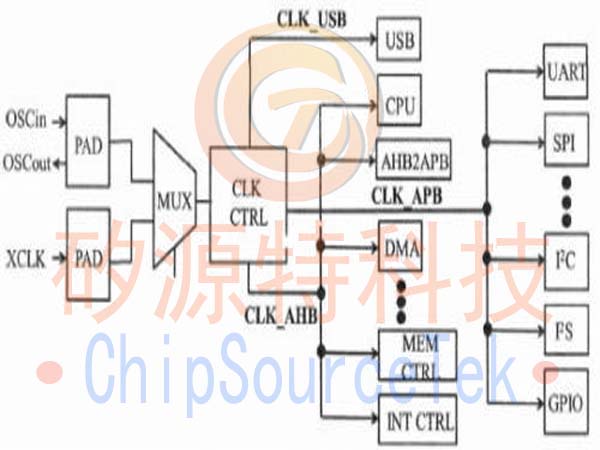
Clock and reset play a crucial role in the entire circuit. If there is a problem with these two signals, the circuit cannot function properly. Therefore, a detailed clock plan and reset plan need to be developed, and different clocks need to be provided for different peripherals: a separate clock for USB, a clock for high-speed peripherals such as CPU, and a clock for low-speed peripherals such as UART, as shown in Figure 1.
Figure 1 Schematic diagram of clock scheme
(3) Bus Scheme Design
The choice of bus, combination method, and number of buses are related to the performance of MCU. Taking the AMBA bus as an example, the usual usage is to connect AHB to high-speed peripherals, and then access low-speed peripherals through the AHB to APB bus bridge. Sometimes, in order to improve the access speed of peripheral devices, there may be two APB buses inside an MCU; There may also be two AHB buses. Separate instructions and data, one for data transmission or image processing, and the other for general control. There may also be a multi-layer AHB interconnection matrix, which allows multiple masters to access multiple different high-speed peripherals simultaneously, greatly improving the performance of the MCU system. Therefore, the development of bus solutions must be determined based on the specific application of the product.
(4) Design of Power Management Scheme
Low power consumption is one of the prominent characteristics of MCU, as it integrates various low-power management strategies: not only does it logically adopt clock gating and gate level optimization methods, but also physically adopts multiple threshold voltages, multiple power domains, gated power supplies, and other methods; At the same time, multiple modes have been adopted in terms of functional modes: normal operation mode, sleep mode, deep sleep mode, power down mode, etc., and strict regulations have been established on the types of IP cores to run and close in each mode, as well as the entry and exit processes between each mode. This ensures both the functionality of the circuit and its performance.
(5) Design of interrupt handling scheme
Interruption is a very important function of MCU. Through interrupt control, the CPU can quickly respond to requests from peripherals. Interrupt processing generally includes the number and priority of interrupt sources, whether they can be masked, whether they are general interrupts or fast interrupts, etc. It is usually necessary to design a dedicated module for interrupt processing. Sometimes, in order to improve design efficiency, IP vendors also provide standard IP cores based on bus interface protocols such as AHB or APB. If this type of IP core can meet the system‘s requirements for interrupt handling, it can also be selected.
(6) Design of Memory Management Scheme
Memory is a larger module in MCU. A MCU may contain three types of storage: ROM, SRAM, and FLASH: ROM is used to store Boot Loaders, IP Drivers, etc. SRAM is used to improve software running speed, store temporary data, and FLASH is used to store application programs and data. Due to the slow read and write speed of FLASH, in order to improve its read and write speed, prefetch buffers and write buffers can be used to accelerate the buffering of instructions and data. Due to each storage having its own address space, it is very convenient for users to access. In order to facilitate system management, a memory management module is usually designed and corresponding control registers are designed in the system control module.
(7) Online debugging scheme design
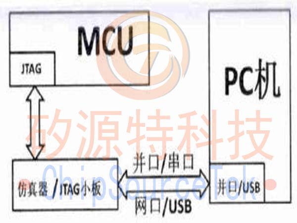
At present, the commonly used online debugging method is serial debugging, such as JTAG, EJTAG, UART, etc., which uses the parallel, serial, network, or USB interfaces of a PC to make online debugging simple, convenient, and cost-effective, as shown in Figure 2. Due to the fact that the debugged program needs to run on the target board and the MCU must function properly, a dedicated debugging module needs to be designed to ensure that the upper computer software can call the CPU for online debugging of software and hardware, and comply with the protocol standard of IEEE1149.1. The basic structure of this module is shown in Figure 3.
Figure 3 Schematic diagram of debugging structure
(8) Test Plan Design
The testing plan for MCU mainly includes physical testing, functional testing, and performance testing. Firstly, perform a clock test on the MCU based on the clock scheme and reset scheme to ensure that the clock circuit is working properly; Perform functional testing on the CPU again, as it is the control core of the MCU, and only when the CPU is running correctly can other IP cores be tested; Then, according to the design specifications, perform functional and performance tests on the digital IP core and analog IP core on the periphery of the MCU.
5.2 System level validation
In order to ensure the correctness of the design, full Functional verification must be performed on MCU before streaming. Therefore, it is necessary to use multiple IIPs and VIPs to build a system level verification platform, develop a detailed verification plan based on the design specifications, use simulation tools, use targeted and random methods or popular validation methodologies such as OVM, VMM, and UVM, and verify the correctness of all MCU functions one by one IP core. The focus is on non-standard modules customized for system functions such as system control units, bus arbiters, and power management.
5.3 FPGA Prototype Verification
Due to the use of EDA tools for software simulation in system level verification, the simulation speed is relatively slow. Therefore, FPGA prototype verification can be used to accelerate the speed of system level verification, especially for modules with complex functions and large scales that need to be downloaded to FPGA. Additionally, larger scale FPGAs such as Virtex 7 series and ArriaV series should be used as much as possible. When building an FPGA verification platform, not only can one FPGA be used, but multiple FPGAs can also be used. It is best to download all the designed modules into the FPGA. FPGA prototype verification not only verifies the correctness of the hardware, but also verifies the correctness of the IP core driver, and can also verify the correctness of the target application.
5.4 Physical Design
After the MCU system level verification and FPGA prototype verification, physical design is required: formulate reasonable design constraints according to the design specification, from logical synthesis to automatic layout and routing, to physical verification, formal verification, Static timing analysis and Functional verification, complete the conversion process from RTL to GDSII, and finally send the data to the OEM for processing and manufacturing.
5.5 Document Design
Documentation is an important and necessary part of the MCU design process, and it should be specified in the form of templates at different stages of design to complete the document design at this stage. The project leader should conduct a detailed review to ensure that once any problems arise in the design, relevant design files and corresponding design documents can be found, especially the details of the design need to be fully reflected.
6 Conclusion
The above is only a brief overview of the main aspects of MCU hardware design. If you want to design a MCU with high cost performance and strong competitiveness, you need to do a lot of detailed work, especially the full Functional verification and detailed testing of the circuit, and build a MCU platform to develop a series of products, so as to ensure that products can continuously enter the embedded market.
|
Disclaimer: This article is transferred from other platforms and does not represent the views and positions of this site. If there is any infringement or objection, please contact us to delete it. thank you!
中恒科技ChipHomeTek
|

 Service mailbox
 13823783658
 ChatNow