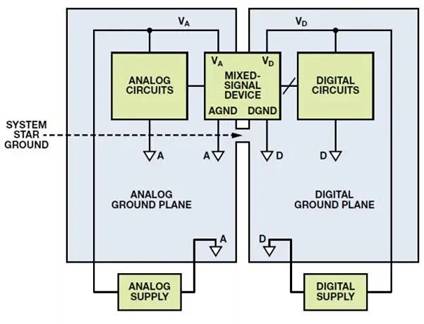
Figure 1 Mixed signal IC grounding: single PCB (typical evaluation / test board)
In this way, the system "Star" grounding is basically generated on the mixed signal device. All high noise digital currents flow into the digital ground plane through the digital power supply, and then return to the digital power supply; Separate from the sensitive analog part of the circuit board. The star grounding structure of the system appears at the position where the analog and digital grounding layers are connected together in the mixed signal device.
This method is generally used in simple systems with single PCB and single ADC / DAC, and is not suitable for multi card mixed signal systems. In systems with several ADCs or DACs on different PCBs (even on the same PCB), analog and digital grounding layers are connected at multiple points, making it possible to establish grounding loop, while single point "Star" grounding system is impossible. In view of the above reasons, this grounding method is not suitable for multi card system. The above method should be used for mixed signal IC with low digital current.
Grounding and decoupling of mixed signal IC with low digital current
Sensitive analog components, such as amplifiers and reference voltage sources, must be referenced and decoupled to the analog ground plane. ADCs and DACs (and other mixed signal ICs) with low digital current should generally be regarded as analog elements, which are also grounded and decoupled to the analog ground plane. At first glance, this requirement seems contradictory because converters have analog and digital interfaces and usually have pins designated as analog ground (agnd) and digital ground (DGND). Figure 2 helps to explain this dilemma.
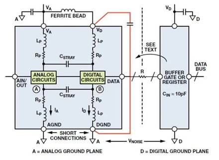
Figure 2 Correct grounding of mixed signal IC with low internal digital current
Inside an IC (such as ADC or DAC) with both analog and digital circuits, the grounding is usually kept independent to avoid coupling digital signals into the analog circuit. Figure 2 shows a simple converter model. Connecting the chip pad to the package pin will inevitably produce wire welding inductance and resistance. IC designers can‘t do anything about it. Just be clear in mind. The rapidly changing digital current generates a voltage at point B and is bound to be coupled to point a of the analog circuit through the stray capacitor cstray. In addition, there is a stray capacitance of about 0.2 pf between each pair of adjacent pins in the IC package, which is also unavoidable! The task of IC designers is to eliminate this influence and make the chip work normally.
However, in order to prevent further coupling, agnd and DGND should be connected externally through the shortest lead and connected to the analog ground plane. Any additional impedance in the DGND connection will generate more digital noise at point B; In turn, more digital noise is coupled to the analog circuit through stray capacitance. Please note that connecting DGND to digital ground plane will impose vnoise on both ends of agnd and DGND pins, causing serious problems!
The name "DGND" indicates that this pin is connected to the digital ground of the IC, but it does not mean that this pin must be connected to the digital ground of the system. It can be more accurately referred to as the internal "digital loop" of IC.
This arrangement may indeed bring a small amount of digital noise to the analog ground plane, but these currents are very small and can be minimized as long as it is ensured that the converter output does not drive a large fan out (which is usually not designed as such). Minimizing the fan out on the digital port of the converter (which also means lower current) can also make the logic conversion waveform of the converter less affected by ringing, and reduce the digital switching current as much as possible, so as to reduce the coupling to the analog port of the converter. By inserting small lossy ferrite beads, as shown in Figure 2, the logic power pin (VD) can be further isolated from the analog power supply. The internal transient digital current of the converter will flow in the small loop from VD to DGND through the decoupling capacitor (this path is represented by the red line in the figure). Therefore, the transient digital current will not appear on the external analog ground plane, but is limited to the loop. The VD pin decoupling capacitor should be installed as close to the converter as possible to minimize parasitic inductance. Decoupling capacitors shall be of the low inductance ceramic type, usually between 0.01 μ F (10 NF) and 0.1 μ F (100 NF).
Again, no one grounding scheme is suitable for all applications. However, by understanding the options and advance rules, you can minimize problems.
|
Disclaimer: This article is transferred from other platforms and does not represent the views and positions of this site. If there is infringement or objection, please contact us to delete. thank you!
中恒科技ChipHomeTek
|

 Service mailbox
 13823783658
 ChatNow