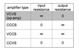
"We know that the amplified voltage can be supplied to the load without attenuation, and the voltage of the signal source will not decay. Therefore, we hope to provide infinite input resistance and zero output resistance for the voltage controlled voltage source. The input resistance and output resistance required by the other three amplifiers are summarized in the table in Figure 2. When divided into the above four types of amplifiers, the operational amplifier is a voltage controlled voltage source. Therefore, the High input resistance and low output resistance are preferred for operational amplifiers with circuit configurations close to this characteristic.”
What is an operational amplifier / comparator?
Amplifier (voltage amplifier) and operational amplifier model
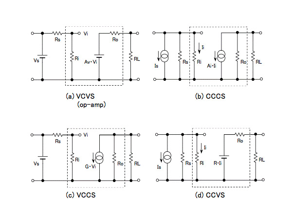
The amplifier has the function of increasing the input signal to output through the amplification factor of the amplifier. Electrical / electronic circuits mainly use voltage and current as input and output signals. The configuration of this amplifier circuit is divided into the following four types:
• VCVS (voltage controlled voltage source) voltage input / voltage output
• CCCS (current controlled current source) current input / current output
• VCCS (voltage controlled current source) voltage input / current output
• CCVs (current controlled voltage source) current input / voltage output
The functions required by the above four types are to detect and amplify the input signal without attenuation, and to provide the output signal without attenuation of the load. We will consider the functions required by the amplifier by modeling the input signal source, amplifier and load. Figure 1 (a) – (d) shows the model of the above four amplifiers, including the input signal source and load. Figure 1 (a) shows the voltage controlled voltage source model. The input resistance of the amplifier is expressed in RI, the output resistance is expressed in RO, and the amplification factor is expressed in AV. The input signal source is modeled by voltage source vs, output resistance Rs and load RL. Using these models, the output voltage is calculated by the following equation:
Vo=(RL/(Ro+RL))·Av·(Ri/(Rs+Ri))·Vs (1.1.1)
The signal voltage is divided by RS and RI to input the attenuated signal to the amplifier. The output voltage of the amplifier is divided by RO and RL and supplied to the load. The larger the RI, the smaller the attenuation of the signal voltage input to the amplifier; The smaller the RO, the smaller the attenuation of the output voltage supplied to the load.
Assuming that RI = ∞ [Ω] and RO = 0 [Ω] in formula (1.1.1), then
Vo=Av·Vs (1.1.2)

 Service mailbox
 13823783658
 ChatNow