Abstract: This paper designs and implements a narrow pulse small signal operational amplifier circuit. At the beginning of the article, it first introduces the use background of the operational amplifier and the purpose of this design, then introduces the design idea and specific circuit implementation, and finally tests the operational amplifier. The test shows that the op amp can amplify the narrow pulse small signal with the rising edge of 50ns.
Operational amplifier is a circuit unit with high magnification. In the actual circuit, the feedback network is usually combined to form a functional module. Because it was used in analog computers in the early stage to realize mathematical operations, it was named "operational amplifier" Operational amplifier is a circuit unit named from the perspective of function, which can be realized by discrete devices or in semiconductor chips. With the development of semiconductor technology, most operational amplifiers exist in the form of single chip. There are many kinds of operational amplifiers, which are widely used in the electronic industry.
This paper introduces a differential operational amplifier composed of three chips in cascade. This operational amplifier can realize narrow pulse small signal amplification, and the rising edge of the pulse can reach 50ns
1 design purpose
According to the needs of the project, the differential operational amplifier designed this time is used to amplify the signal output by the detector. Because the signal received by the receiver is small signal pulse modulation, the designed operational amplifier must be able to amplify narrow pulses of large and small signals. Because in the case of small signal, the output of the detector is at the millivolt level, and the index requires the output to be between -2~+2v, the amplification factor of the designed differential amplification circuit is about 100 times.
2 design idea
Since the operational amplifier designed this time is to amplify the pulse signal, the problem of the rising edge of the pulse signal must be considered. If the rising edge time is too long, resulting in the distortion of the pulse signal, the initial design is to limit the rising edge time of the pulse signal t<50ns Because the bandwidth and rising edge of the pulse signal have the following relationship: F × T=3.5 (f means bandwidth). It can be seen that the smaller the rising edge time is, the larger the bandwidth is. When the rising edge time is t=50ns. The bandwidth will reach 70MHz Because the bandwidth of the operational amplifier is inversely proportional to the gain, if only one stage of the operational amplifier is used, the gain will not reach the required 100 while reaching the required bandwidth. Therefore, the operational amplifier designed this time adopts a two-stage amplification structure, with each stage amplified by 10 times.
3 related circuit
From the above analysis, we can see that this op amp circuit adopts a two-stage structure. At the first stage, the baseband signal is differential amplified. The chips are ada4817-1 and ada4817-2 of ad company. The first stage amplification circuit is shown in Figure 1.
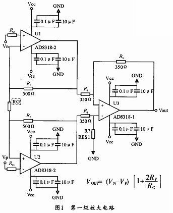
The chips ada4817-1 (single channel) and ada4817-2 (dual channel) fastfet amplifiers used in the first stage amplification are unit gain stable, ultra-high speed voltage feedback amplifiers with FET input. These amplifiers adopt ADI‘s proprietary ultra-high speed complementary bipolar (xfcb) process, which enables the amplifier to achieve high speed and ultra-low noise (4nv/ √ Hz; 2.5 fa/ √ Hz) and extremely high input impedance.
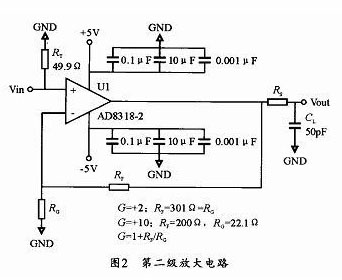
The signal output from the first stage is amplified twice, and the ad8009 chip of ad company is selected for the second stage amplification. Figure 2 shows the second stage amplification circuit.
The chip ad8009 used in the second stage amplification is an ultra-high speed current feedback amplifier with a staggering swing rate of 5500 v/ μ s. The rise time is only 545ps, so it is very suitable for use as a pulse amplifier.
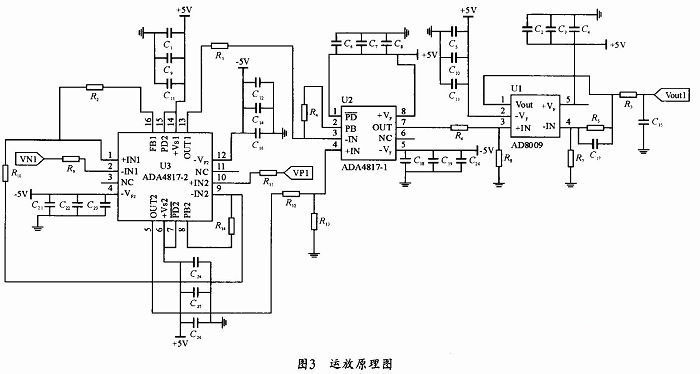
In addition, in order to prevent self excitation, a 10 Ω resistor is connected between the two stages of amplification. Figure 3 is the overall schematic diagram of the differential operational amplifier.
4 Conclusion
To sum up, it shows that the operational amplifier amplifies the millivolt level narrow pulse small signal output by the detector nearly 100 times without distortion. This proves that the differential operational amplifier designed this time can meet the requirements and has good performance.
|
Disclaimer: This article is transferred from other platforms and does not represent the views and positions of this site. If there is infringement or objection, please contact us to delete. thank you!
中恒科技ChipHomeTek
|

 Service mailbox
 13823783658
 ChatNow