The structure of voltage and current feedback amplifier application circuit is generally the same, except for several key points.
The current feedback amplifier has a higher conversion rate than the voltage feedback amplifier. In this way, current feedback amplifier can solve high-speed problems better than voltage feedback amplifier. The name of "current feedback amplifier" has some mystery, but generally, the structure of the application circuit of current feedback amplifier and voltage feedback amplifier is the same, except for several key points.
First, the feedback resistance of the current feedback amplifier circuit must be kept within a small range. The lower the resistance, the worse the stability of the current feedback amplifier. The specified resistance value can be found in the current feedback amplifier product manual. The feedback resistance value of the voltage feedback amplifier is wider. The driving ability of the amplifier limits the minimum value of the resistance, and the noise of the whole circuit limits the maximum value of the resistance.
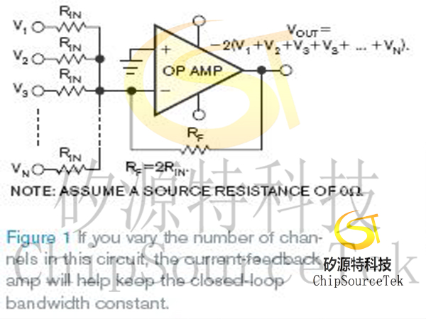
Figure 1 shows a circuit suitable for current or voltage feedback amplifiers. If the feedback resistance RF is equal to 2rin, where Rin is the input resistance, and the closed-loop gain of each channel is – 2v/v. At first glance, it is easy to assume that the product of closed-loop bandwidth and gain bandwidth divided by the gain of each channel is equal, or | - 2v/v |. But don‘t make this assumption!
Figure 1 shows a circuit suitable for current or voltage feedback amplifiers. If the feedback resistance RF is equal to 2rin, where Rin is the input resistance, and the closed-loop gain of each channel is – 2v/v. At first glance, it is easy to assume that the product of closed-loop bandwidth and gain bandwidth divided by the gain of each channel is equal, or | - 2v/v |. But don‘t make this assumption!
If the voltage or current feedback amplifier in the circuit shown in Figure 1 is used, the noise gain is:
Where n is the number of input channels. The circuit bandwidth with voltage feedback amplifier is equal to the gain bandwidth product divided by the noise gain. For example, if a voltage feedback amplifier with 180mhz gain bandwidth product is used, there are three input channels (n=3), the gain is – 2v/v, and the closed-loop bandwidth of the circuit is 25.7 MHz. Additional channels reduce the closed-loop bandwidth, even if the input signal continues to achieve a gain of – 2v/v.
If the current feedback amplifier as shown in Figure 1 is used, the closed-loop bandwidth of the amplifier depends less on the closed-loop gain and the number of input channels. If you use such an amplifier to design the circuit, you should first choose the appropriate feedback resistance, the specifications of each manufacturer and the noise gain of the circuit. Then select the appropriate Rin value. From this point, if the circuit increases the channel, there may be small changes in the signal bandwidth and gain. If that happens, go back and determine the choice of feedback resistance. For current and voltage feedback amplifiers, the noise gain is usually equal to the result of Formula 1, but reducing the feedback resistance of the current feedback amplifier circuit increases the circuit bandwidth.
|
Disclaimer: This article is transferred from other platforms and does not represent the views and positions of this site. If there is infringement or objection, please contact us to delete. thank you!
中恒科技ChipHomeTek
|


 Service mailbox
 13823783658
 ChatNow