In the first part, we explained how to choose the correct capacitor type, power inductor, switching frequency and semiconductor, which are important to the efficiency of dc/dc switching controller, and showed examples of the task of developing step-down and step-up converters with specified specifications. We also discussed how to choose the best capacitor and inductor to create a filter that matches the converter, so as to achieve very low inductance and compact layout. In part 2, we will introduce the factors that need to be considered for circuit board layout and EMC, the selection of input and output filter components, and the use of thermal imaging to verify functional circuits.
Layout guide
Some factors need to be taken into account when laying out the circuit board. For example, high Δ I/ Δ The input and output circuits of T value should be kept compact by placing filter ceramic capacitors closely together. The bootstrap circuit should be compact and close to the switching regulator IC. A wide-band π filter is needed to decouple the internal power supply of the switching regulator. Use as many vias as possible to realize the low inductance and low impedance connection between the internal power GND layer and the bottom layer of the circuit board. Although a large area of copper can achieve better heat dissipation performance and lower RDC, the copper area should not be too large to avoid capacitive and inductive coupling with adjacent circuits.
EMC measurement without filter (100W output power).
In order to meet most applications, the interference emission of the converter in the range of conduction (150kHz to 30MHz) and radiation (30MHz to 1GHz) should comply with class B (household) limits. In addition to insertion loss, it is also important that high current applications require inductive components to have the lowest possible RDC, so as to maintain efficiency and calorific value within an acceptable range. Unfortunately, low RDC also means larger size. Therefore, it is particularly important to choose the most advanced components that balance RDC, impedance and size. We-mpsb series and compact design we-xhi series are suitable for this situation. For capacitive filter elements above 10 µ F, low-cost aluminum electrolytic capacitors can be used. Since the filter inductor can effectively suppress current changes, there is no need to worry about high ripple current. Therefore, a larger ESR does not matter. It will reduce the quality factor of the filter, so as to prevent unnecessary resonance. The additional loss caused by the filter is due to the ohmic loss of the inductor.
Select input and output filter elements
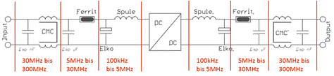
The most important point in the filter element selection standard is to realize broadband interference suppression from 150kHz to 300MHz, so as to suppress conducted and radiated EMC. If the input or output uses a shorter cable or does not use a cable, the filtering degree can be reduced. Figure 6 shows the effective frequency range of each filter element.
Figure 6: block diagram of filter elements with three different frequency ranges.
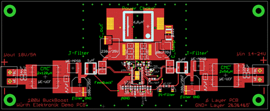
Figure 7: top view of PCB, including all filter elements, meeting cispr32 class B standard
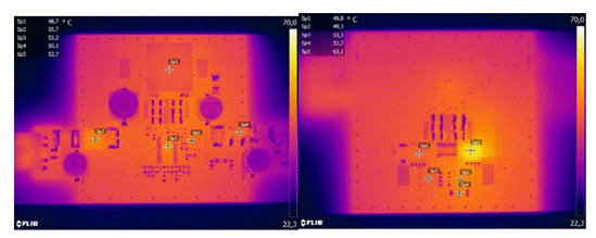
Measured temperature and efficiency of circuit with filter at 100W output power (TA = 22 ° C)
The maximum temperature of the components measured by the thermal imager is lower than 64 ℃ (Fig. 8), which means that there is enough safety margin to cope with the higher ambient temperature, and the pressure on the components is also small. The efficiency is also at a very high level (buck mode: 96.5%; boost mode: 95.6%), especially considering that all filter elements have been included.
Figure 8: temperature measured at the top and bottom.
Figure 9: radiated interference emissions measured by circuits with filters at the input and output. It can keep enough distance from the limit value (horizontal and vertical) in the whole measurement range.
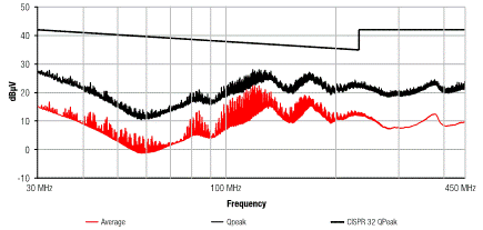
Figure 10: measured conducted emissions with a filter at the input. The average value and quasi peak value are lower than the limit value in the whole measurement range.
Figure 9 and figure 10 show the improvement of circuit measurement results after installing the filter. With the filter, the peak value of conducted interference radiation in the low frequency range and the complete measurement curve of radiated interference emission are lower than the required limit, and there is sufficient margin.
summary
Even if the layout is very careful and the appropriate active and passive components are selected, if there are additional very strict specification requirements (such as long cables, no shielding, etc.), the high-power dc/dc converter that meets the class B standard cannot be realized without the filter. However, we can expect and arrange appropriate filters in advance. The result is a flexible, efficient 100W step-down and boost converter that meets the class B standard. In order to make the printed circuit board more compact, the two filters can be rotated by 90 ° or arranged on the opposite side of the circuit board. Design and simulation software such as redexpert and LTSpice help to achieve the desired design goals quickly and cost effectively.
Author:
Andreas Nadler, field application engineer of WuErTe electronics, FAE, appnotes@we-online.de ,
|
Disclaimer: This article is transferred from other platforms and does not represent the views and positions of this site. If there is infringement or objection, please contact us to delete. thank you!
中恒科技ChipHomeTek
|


 Service mailbox
 13823783658
 ChatNow