In the switching power supply, the superposition of AC ripple in the stable DC signal is usually a problem that engineers worry about. So how can we reduce and suppress the ripple noise?
What is power ripple and how is it generated?
With the development of switching power supply, more and more traditional linear power supply has been replaced by its superior performance. However, the output ripple of switching power supply has always been a headache for engineers. What is the power ripple and how is it generated? We know that the DC voltage output by the switching power supply is obtained by rectifying, filtering and stabilizing the AC voltage. Due to the unreasonable design of the filter circuit in the circuit, there will be periodic and random clutter above the DC level, which will generate ripple. In the case of rated output voltage and current, the peak value of the AC voltage in the output DC voltage is commonly referred to as the ripple voltage. In short, ripple is the AC component superimposed on the stable DC output.
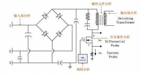
Figure 1 main structure of switching power supply
Methods of testing power ripple and restraining power ripple
The ripple carried in the switching power supply will reduce the use efficiency of the power supply, the higher ripple may also generate surge voltage or current, and in the digital circuit, the ripple will also interfere with the logic level relationship of the circuit, which is harmful; In the design of switching power supply, we not only need to measure the ripple correctly, but also reduce the ripple as much as possible.
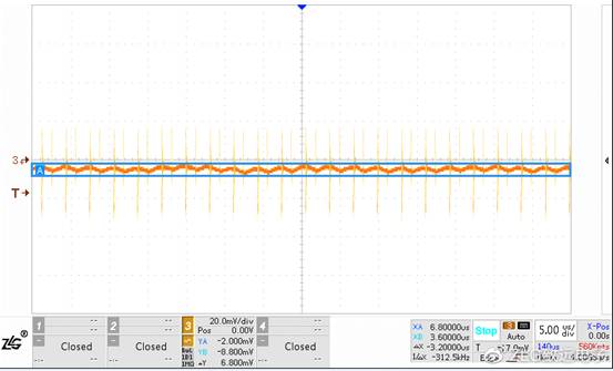
The correct method for measuring ripple usually requires the following steps:
1. First, the probe should select the appropriate gear. In general, it is recommended to use the X1 gear to avoid unnecessary noise attenuation affecting the measurement of ripple;
2. Select the channel coupling mode as AC coupling to limit the input of DC signal;
3. Open the "bandwidth limit" function of the oscilloscope and select the "20MHz" bandwidth limit to filter out unnecessary high-frequency noise;
4. In order to avoid interference of electromagnetic radiation and other signals, it is recommended to use "grounding spring" for grounding during measurement to avoid unnecessary interference caused by long grounding wire;
5. Adjust the horizontal time base, vertical gear and offset so that the ripple signal is displayed in the center of the screen (the blue frame in Fig. 2 shows the oscilloscope ripple test results).
Fig. 2 oscillograph test ripple results
In order to effectively reduce ripple, the circuit design can be improved from the following aspects:
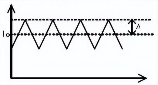
1. Increase inductance or switching frequency
According to the formula of the switching power supply, the current fluctuation in the inductor is inversely proportional to the inductance value. The switching frequency can be increased to reduce the energy transmitted each time to reduce the ripple (but increasing the switching frequency will also increase the switching loss), or the inductance value L of the energy transmitted can be increased to reduce the abrupt peak value of the current and reduce the ripple amplitude.
Fig. 3 current waveform in inductance
2. Increase capacitance
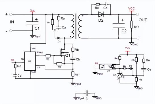
Since the output ripple is inversely proportional to the output capacitance, the output filter capacitance can be increased to reduce the ripple, and the capacitance cannot be increased indefinitely. Most switching power supply modules have the maximum capacitive load limit. The capacitor C or RC (as shown in Fig. 4, D2 and Q1) can also be connected to the diode and the switch tube. When the diode is turned on and off at high speed, the equivalent inductance and the equivalent capacitance become an RC oscillator during the reverse recovery of the diode to generate high-frequency oscillation. In order to suppress this high-frequency oscillation, a capacitor C or RC buffer network should be connected in parallel at both ends of the diode. The resistance is generally 10 Ω - 100 Ω, and the capacitance is 4.7pf-2.2nf.
Figure 4 switching power supply circuit
3. After switching power output, add voltage regulator
Adding a low dropout linear regulator (LDO) after the output of switching power supply or module power supply can greatly reduce the output noise to meet the needs of circuits with special noise requirements, and the output noise can reach μ Class v. Since the voltage difference of LDO (difference between input and output voltage) is only several hundred MV, the standard voltage can be output when the output of switching power supply is slightly higher than that of LDO by several hundred MV, and the loss is not large.
4. Standard PCB wiring
There may be multiple module power supplies working together on the same PCB. If the module power supply is not shielded and is close to each other, it may interfere with each other to increase the output noise voltage. In order to avoid such mutual interference, shielding measures can be taken or they can be properly kept away to reduce the mutual interference. For example, two output capacitors can be used, one close to the rectifier tube and the other close to the output terminal. The parallel connection effect of two small capacity capacitors is better than that of one large capacity capacitor. The parallel connection of multiple capacitors can improve the high-frequency impedance characteristics of the capacitor.
summary
In the power supply design, the above-mentioned methods can be used to reduce the ripple, but the advantages and disadvantages coexist more or less. It is necessary to weigh the points that need to be improved most to select the appropriate scheme. Of course, it is also possible to select the ready-made stable finished power supply, in which the filter circuit and isolation part have been highly integrated.
|
Disclaimer: This article is transferred from other platforms and does not represent the views and positions of this site. If there is infringement or objection, please contact us to del
中恒科技ChipHomeTek
|

 Service mailbox
 13823783658
 ChatNow