Many applications require the use of low-power, high-performance differential amplifiers to convert small differential signals into readable ground reference output signals. The two inputs usually share a large common mode voltage. The differential amplifier will suppress the common mode voltage, and the residual voltage will appear as a single terminal voltage at the output of the amplifier after amplification. The common mode voltage may be an AC or DC voltage, which is usually greater than the differential input voltage. The suppression effect decreases as the common mode voltage frequency increases. Amplifiers in the same package have better matching performance, the same parasitic capacitance, and do not need external wiring. Therefore, compared with the discrete amplifier, the dual channel amplifier with high performance and high bandwidth has better frequency performance.
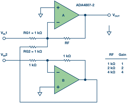
A simple solution is a dual channel precision amplifier using a resistive gain network, as shown in Figure 1. This circuit shows a simple way to convert a differential input to a single ended output with adjustable gain. The system gain can be determined by Formula 1:
Where gain = RF / 1K and (vin1 – vin2) is the differential input voltage.
Figure 1. Differential input single ended output amplifier.
In general, this method can provide more stable reading function in case of EMI or RFI. Therefore, it is recommended to use it in case of noise problems. This is especially true when measuring thermocouple, strain gauge and bridge type pressure sensor inputs because they can provide very small signals in noisy environments.
This circuit can not only measure the voltage difference between the positive and negative terminals of the sensor, but also provide the common mode suppression function with partial system gain, and achieve better performance improvement than single terminal input. In addition, the sensor ground may be different from the analog ground. Ground output voltage reference is very important in many applications. The system depends on the tolerance of the network resistance.
The circuit can convert the differential input into a single ended output with adjustable gain. The system gain can be set by the ratio of RF and Rg1, assuming that Rg2 = Rg1 and the gain of amplifier B is - 1.
For example, the 180mhz dual channel amplifier ada4807-2 can be constructed as an inverting amplifier for this application, and the noise of this circuit is low. This circuit has a low static current (1000A / amplifier), which is suitable for low power consumption and high resolution data conversion system.
The input common mode voltage will be higher than the supply voltage. Rail to rail output is adopted, which is very useful in large common mode signal or large output voltage applications. For example, the data acquisition board has an ADC that can accept 0V to 5V single ended input. However, the signal source happens to be the differential voltage generated by the sensor bridge. One terminal of the bridge is positive and the other terminal is negative to respond to the pressure in the presence of common mode noise.
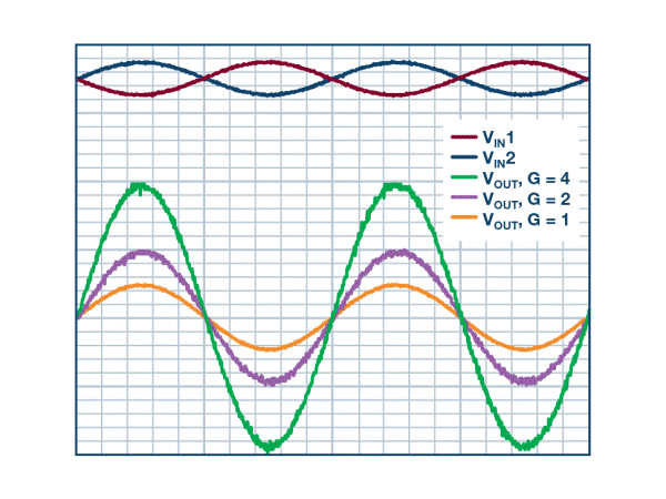
Figure 2. Performance of differential to single ended amplifier.
Fig. 2 shows the case where the differential input voltage is applied and the circuit gain changes. The RF value sets the system gain. It can be seen that this figure shows the system gains 1, 2 and 4, and the differential input voltage at 1kHz is 1vp-p.
This circuit is very useful for measuring small differences between two large voltages. For example, a solution can be considered to monitor a typical Wheatstone bridge circuit powered by 3V / GND in a 3V battery powered system with a 1% simplicity. The required level can be achieved by using 1% resistance or better, and this circuit will suppress any common mode and amplify and attenuate the bridge signal according to the set circuit gain. If the ADC is driven, some level conversion functions need to be applied to obtain an output signal in the range of 0V to 5V.
The circuit has excellent distortion and low quiescent current. The dual channel operational amplifier solution can reduce the system cost, while the use of differential amplifiers can improve the performance.
|
Disclaimer: This article is transferred from other platforms and does not represent the views and positions of this site. If there is infringement or objection, please contact us to del
中恒科技ChipHomeTek
|


 Service mailbox
 13823783658
 ChatNow