Figure 5. Through hole connection.
Please note that the following parameters about vias and PCB rails: rail width, vias size and electrical parameters are affected by several factors, such as PCB coating, routing layer, operating temperature, etc. These factors will eventually affect the current carrying capacity. Previous PCB design techniques did not consider these dependencies, but designers need to pay attention to these when determining layout parameters. At present, many PCB rail/via calculators can be used online. After completing the schematic design, the designer should consult the PCB manufacturer or layout engineer for these details.
Avoid overheating
There are many factors that can cause heat generation, such as housing, airflow, etc., but this section focuses on exposed pads. Controllers with exposed pads, such as LTC3533, ADP5304, ADP2386, ADP5054, etc., will have lower thermal resistance if properly connected to the circuit board. Generally speaking, if the power MOSFET of the controller IC is placed in the die (i.e., the whole chip), the bonding pad of the IC is usually exposed for heat dissipation. If the converter IC operates with an external power MOSFET (controller IC), the control IC usually does not need to use an exposed pad, because its main heat source (power MOSFET) itself is external to the IC.
Generally, these exposed pads must be welded to the PCB ground plate to be effective. There are some exceptions according to the different ICs. Some controllers will indicate that they can be connected to the isolated PCB area of the pad for heat dissipation. If in doubt, refer to the data sheet for the component.
When you connect exposed pads to a PCB plane or isolated area, (a) ensure that these holes (many arranged in an array) are connected to the ground plane for heat dissipation (heat transfer). For multilayer PCB ground planes, it is recommended to use vias to connect the ground planes on all layers below the pad.
Note that the discussion of exposed pads is related to the controller. Using exposed pads in other ICs may require a very different approach.
Conclusion and summary
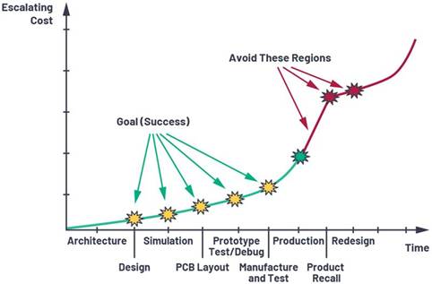
To design a low noise power supply that will not affect the system circuit due to rail or via burning, it is a challenge in terms of cost, efficiency, efficiency and PCB area. This article highlights some areas that designers may ignore, such as using power budget analysis to build a power tree to support all back-end loads.
Schematic diagram and simulation are only design steps, followed by careful device positioning and routing technology. The through-hole, rail and current carrying capacity must meet the requirements and be evaluated. If there is switching noise at the interface position, or the switching noise reaches the power pin of the IC, the system circuit will be out of order, and it is difficult to isolate and troubleshoot.


 Service mailbox
 13823783658
 ChatNow