There are many different switching regulator topologies. Some topologies are widely used, such as the classic buck converter, also known as the buck converter. However, there are also some little-known switching mode DC-DC converters, including Zeta topologies. These topologies are divided into basic topology and extended topology. The basic topology only uses two switches, one inductor and two capacitors. They are non isolated switching regulators; That is, switching voltage regulators that are not electrically isolated. Such topologies include step-down converter, step-up converter and inverse step-down step-up topology. All other topologies require additional components. For example, the SEPIC converter also requires a coupling capacitor and a second inductor. In addition to non isolated switching regulators, some regulators are electrically isolated through transformers.
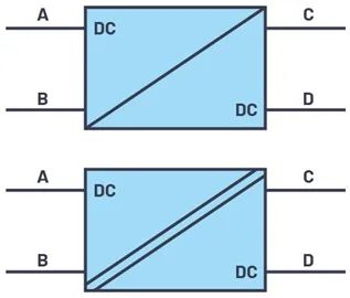
Circuit designers usually regard power supply as a black box or a 4-pole component. It has two input lines and two output lines. Figure 1 shows the block diagram symbol of DC-DC converter. The top is a non electrically isolated DC-DC converter, and the bottom is an electrically isolated converter.
Figure 1. The switch mode power supply is displayed as a black box.
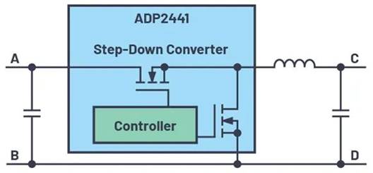
The noise characteristics of terminals are not shown in Figure 1. Different switching regulator topologies have different noise characteristics at the 2-port network terminals. Figure 2 shows the ADP2441 general-purpose buck converter for industrial applications. It can convert 24 V input voltage to 3.3 V output voltage. When using this topology, it can be seen that the input side will generate pulse current, so the noise is very large. When the high side switch on ADP2441 is on, the current flows into terminal A. When this switch is turned off, no current flows through node A. However, the noise of output C is very small. The inductance in the output path ensures that there is no pulse current at the output end.
Figure 2. Actual switching regulator topology design.
Table 1 summarizes the basic noise characteristics of switching regulators, which provides an important reference for system designers in conceptual design. The most common switching regulator topologies are listed in the table. The first line indicates the noise level of the input (i.e. terminals A and B of the 2-port network). The second line indicates the noise level of the output end of the corresponding topology (i.e. terminals C and D of the 2-port network). Table 1 shows the noise level.
Table 1. Overview of Common Switching Regulator Topologies and Their Input and Output Noise Characteristics
For example, using separate LC filters for additional filtering can significantly reduce conducted noise in switching regulator circuits. In this way, high noise in Table 1 can be avoided. However, the system designer should know which DC-DC converters have high noise at which terminals. In this way, they can pre consider the corresponding filters and the additional space that these filters must occupy.
ADP2441
·Wide input voltage range: 4.5 V to 36 V
·Minimum conduction time: 50 ns
·Maximum load current: 1 A
·High efficiency: up to 94%
·Adjustable output: min. 0.6 V
·Output voltage accuracy: ± 1%
·Adjustable switching frequency: 300 kHz to 1 MHz
·Pulse skip mode under low load, saving power
·Precision enable input pin
·Good indication of open drain power supply
·External soft start with tracking function
·Overcurrent limit protection
|
Disclaimer: This article is transferred from other platforms and does not represent the views and positions of this site. If there is any infringement or objection, please contact us to delete it. thank you!
中恒科技ChipHomeTek
|


 Service mailbox
 13823783658
 ChatNow