Reducing ripple noise at the load end is a common concern for most users in the application of power modules. The following text combines the waveform and testing method of ripple noise, and elaborates on several effective methods to reduce output ripple noise from the perspective of power supply design and peripheral circuits.
1. Figure displaying the ripple and noise of the power supply
Ripples and noise refer to the fluctuations superimposed on the output of a DC power supply that have the same frequency as the power switch frequency, which are called ripples, while high-frequency noise is called noise. As shown in Figure 1, the lower frequency and regular fluctuations are ripples, and the peak part is noise.
Figure 1
2. Testing methods for ripple noise
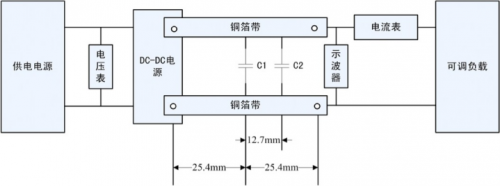
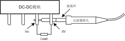
For ripple noise testing of small and medium-sized power module power supplies, the industry mainly adopts two methods: parallel line testing and proximity testing. Among them, the parallel line test method is used for products with relatively large pin spacing, and the relying test method is used for products with small module pin spacing.
However, whether using parallel line testing or relying on measurement methods, it is necessary to limit the bandwidth of the oscilloscope to 20MHz and remove the ground clamp.
As shown in Figures 2 and 3.
Note 1: C1 is a high-frequency capacitor with a capacity of 1 μ F; C2 is a tantalum capacitor with a capacity of 10 μ F.
Note 2: The distance between two parallel copper foil strips is 2.5mm, and the sum of the voltage drops of the two parallel copper foil strips should be less than 2% of the output voltage.
Figure 3 Measurement method
3. Differences in removing ground wire clamp testing
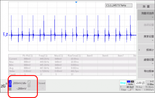
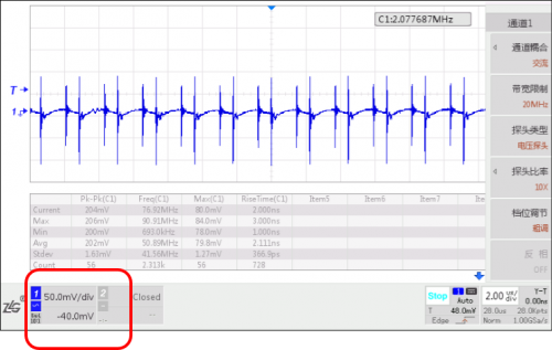
Testing ripple noise requires removing the ground clamp, mainly because the ground clamp of the oscilloscope absorbs various high-frequency noise and cannot truly reflect the output ripple noise of the power supply, which affects the measurement results. Figures 4 and 5 below respectively show the significant differences between using and removing ground clamps for testing the same product.
Figure 4 Using Ground Clamp Test - Oscilloscope Vertical Resolution 200mv/div
Figure 5 Removal of Ground Clamp Test - Oscilloscope Vertical Resolution 50mv/div
4. The impact of PCB layout on design
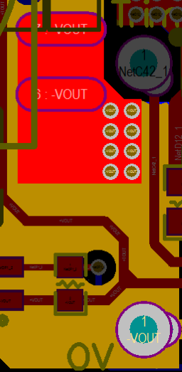
Good and bad PCB layout is a key factor affecting ripple noise in design. The poor PCB layout is shown in Figure 6. The ground output of the transformer is directly connected to the ground plane on the back through a via hole, and the ground plane is connected to the output pin of the power supply. This layout has a measured power peak of 1.5V VP-P under a load output of 5V/2A.
Figure 6 Poor PCB Layout
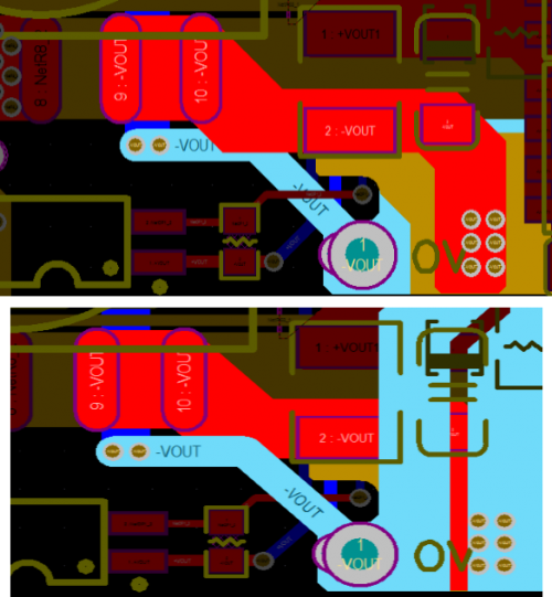
As shown in Figure 7, the PCB layout is relatively good. The position of the transformer has been adjusted, and the output ground of the transformer is passed through two capacitors before returning to the ground plane and connecting to the output pins. The measured noise has decreased to 60mV VP-P under the same 5V/2A output load, with a significant difference.
Figure 7 Good PCB Layout
5. The influence of output filtering capacitance
The capacitance and ESR of the output filter capacitor also have a direct impact on the ripple noise output by the module. Test the ripple noise of the product as shown in Figure 8.
Without external capacitors, the ripple noise output during testing is approximately 100mV, as shown in Figure 9. Under the same input and load conditions, adding 226 MLCC to the output of the power supply reduces the ripple noise of the measured power output to less than 40mV.
Figure 8 Test diagram
Figure 9: No external capacitance
Figure 10: Applied 226 capacitors
In practical applications, in addition to capacitance and ESR, it is recommended that the capacitance at the load end be collected into the output capacitor before returning to the power supply. After capacitor filtering, it is then returned to the power supply, effectively reducing the impact of ripple noise on the circuit. As shown in Figure 11.
Figure 11 Location of External Capacitors
6. The Influence of Inductance on Ripple Noise
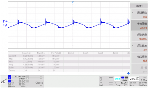
The inductance and parasitic capacitance of the inductor also have a significant impact on ripple noise. Generally, when the inductance is high, the ripple suppression effect is obvious, while inductance with small parasitic capacitance has good noise suppression effect. Taking ripple suppression as an example, test the impact on the output ripple of the power supply, as shown in Figure 12.
Figure 12 Test Case for Inductive Filter Effect
According to Figure 12, we artificially short circuited the filtering inductance inside the product and only used capacitor filtering. The measured ripple noise is shown in Figure 13, with a peak ripple value of about 50mV.
Figure 13 Ripple noise diagram of internal filtering inductance caused by artificial short circuit
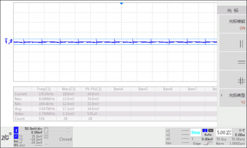
Next, add a LC circuit outside the power supply. Under the same input and load conditions, retest the ripple noise diagram, as shown in Figure 14. The ripple is close to a straight line and very small.
Figure 14 Ripple noise map with additional LC
The above briefly starts with the legend and testing methods of ripple noise, describing several methods for reducing ripple noise starting from power supply design and external circuit applications, combined with actual testing. In practical engineering applications, it is necessary to consider the load effects of capacitors and inductors, self-excited effects, etc., and further investigation is needed.
|
Disclaimer: This article is transferred from other platforms and does not represent the views and positions of this site. If there is any infringement or objection, please contact us to delete it. thank you!
中恒科技ChipHomeTek
|


 Service mailbox
 13823783658
 ChatNow