(1) Pad spacing. If it is a new device, you need to draw the component packaging yourself to ensure the appropriate spacing, as the pad spacing directly affects the soldering of the component.
(2) Through-hole size (if any). For plug-in devices, sufficient margin should be reserved for the through-hole size, generally not less than 0.2mm is more appropriate.
(3) Outline screen printing. The outline screen printing of the device should preferably be slightly larger than the actual size to ensure smooth installation of the device.
2. Layout
(1) IC should not be close to the board edge.
(2) Components of the same module circuit shall be placed close to each other. For example, the Decoupling capacitor should be close to the power supply pin of the IC, and the components constituting the same functional circuit should be placed in one area with clear hierarchy to ensure the realization of functions.
(3) Arrange the location of sockets according to actual installation. Sockets are all led to other modules. According to the actual structure, in order to facilitate installation, the principle of proximity is generally adopted to arrange the position of sockets, and they are generally close to the board edge.
(4) Pay attention to the direction of the socket. Sockets are all directional, and if the direction is reversed, the wires need to be customized. For flat sockets, the direction of the socket should be towards the outside of the board.
(5) Keep Out area cannot have devices.
(6) Disturbance sources should be kept away from sensitive circuits. High speed signals, high-speed clocks, or high current switching signals are all sources of interference and should be kept away from sensitive circuits, such as reset circuits or analog circuits. They can be separated by paving the ground.
3. Wiring
(1) Line width size. The line width should be selected based on the process and current carrying capacity, and the minimum line width cannot be less than the minimum line width of the PCB manufacturer. At the same time, to ensure the carrying current capacity, a suitable line width of 1mm/A is generally selected.
(2) Differential signal line. For differential cables such as USB and Ethernet, it is important to route them equally, parallel, and in the same plane, with the spacing determined by impedance.
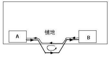
(3) Pay attention to the return path on the high-speed line. High speed lines are prone to electromagnetic radiation. If the area formed by the routing path and the return path is too large, a single turn coil will form to radiate electromagnetic interference outward, as shown in Figure 1. Therefore, when routing, it is important to note that there is a return path next to it, and the multi-layer board with a power layer and ground plane can effectively solve this problem.
(4) Pay attention to the analog signal line. The analog signal line should be separated from the digital signal, and the routing should try to avoid passing by interference sources (such as clocks and DC-DC power supplies), and the shorter the routing, the better.
4. EMC and Signal integrity
(1) Terminate the resistor. It is best to connect a matching resistor at the end of a high-speed line or a digital signal line with higher frequency and longer routing.
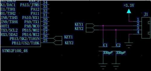
(2) Connect the input signal line to a small capacitor. It is best to connect the signal line input from the interface with a small capacitance of pico level near the interface. The capacitance is determined according to the signal strength and frequency, and cannot be too large, or it will affect the Signal integrity. For low-speed input signals, such as button inputs, a small capacitor of 330pF can be selected, as shown in Figure 2
(3) Driving ability. For example, switching signals with high driving current can be driven by adding a transistor; For buses with large fan outs, a buffer (such as 74LS224) can be added for driving.
Figure 2
5. Silk screen printing
(1) Board name, time, PN code.
(2) Annotation. Label the pins or key signals of some interfaces (such as arrays).
(3) Component label. Component labels should be placed in appropriate positions, and dense component labels can be grouped and placed. Be careful not to place it in the through hole position.
6. Other
Mark point. For PCBs that require machine welding, two to three Mark points need to be added.
|
Disclaimer: This article is transferred from other platforms and does not represent the views and positions of this site. If there is any infringement or objection, please contact us to delete it. thank you!
中恒科技ChipHomeTek
|

 Service mailbox
 13823783658
 ChatNow